Back Scattered Electron Detector : Some of the primary electrons are scattered back and a detector positioned appropriately can be used to collect the information. This is called back scattered electron (BSE) detector. The BSE comes mainly from nuclear interaction. The BSE signal depends on the composition. Hence BSE can be used to obtain information about the composition, but the spatial resolution is not very good.
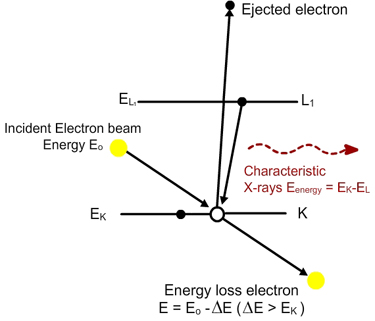
Figure 12. 6. Illustration of energy levels and EELS in TEM
EELS: Sometimes, the primary electrons coming at the other end of the samples can be detected. This is true only when the sample thickness is very small. By measuring the energy loss of the incident electrons, the composition of the material can be determined (Figure 12.6) . This mode of operation can be used for imaging and is called transmission electron microscopy (TEM). When it is used to characterize the chemical nature by measuring the energy of the electron accurately and thus by calculating the energy loss, it is called electron energy loss spectroscopy (EELS).
XPS: A related technique is used to characterize the surface. In this, X rays can be used to probe the sample. The atoms will absorb the X rays and the energy will be emitted as electrons (Figure 12.7) My monitoring the electrons emitted, it is possible to determine the chemical composition. Even the state of ioinization can be determined using this technique. i.e. It can be used to differentiate the chemical state of the atom i.e. Cu(II), vs Cu(I) vs Cu. This is not possible, for example, using EDX technique. Since the emitted electrons are used to determine the chemical composition, this technique is also called ESCA (electron spectroscopy for chemical analysis). A photo of an XPS equipment is shown in Figure 12.8
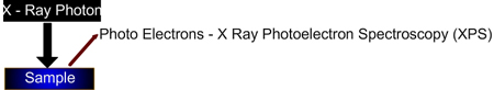
Figure 12.7. Illustration of energy levels and generation of photoelectron in XPS
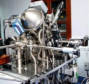
Figure 12.8. A photo of XPS equipment (Courtesy, Prof. T. Pradeep, Dept. Chemistry, IIT-Madras)
Focused Ion Beam: Focused ion beam is similar to the SEM except that instead of electrons, a beam of ions is used. It is frequently used in semiconductor industry for ‘milling’, i.e. cutting the sample for analysis. A metal with low melting point (gallium) is used as a source. When it is placed on a tungsten needle and when a current is applied, gallium melts and flows to the tip. It forms a cone of about 2 nm size and at high electric fields, it ionizes and is emitted. The emitted ions are accelerated and focused, similar to the way the electrons are manipulated in a SEM. It can be used at low currents for imaging and at high currents for milling (i.e. removing the material, in a very small area). If the sample is an insulator, a low energy electron gun can be used to ensure that the surface remains neutral.
The ions are larger than electrons and also much heavier. They do not penetrate deep into the substrate. FIB is inherently destructive, in the sense some of the sample atoms will be removed from the surface and after imaging or milling, some source atoms (i.e. gallium) will be present in the top of the sample surface. Micro machining (i.e. milling with micron sized features) is very common and nano machining (i.e. with 10-15 nm sized features ) is possible.
FIB is particularly useful in failure analysis (i.e. determining the root cause of failure in a chip). When a chip fails, if the approximate location of the failure is determined by some technique or analysis, then using FIB, the chip can be milled to that location and the image of the layers in that location can be acquired using SEM to understand the cause of failure.
Atomic Force Microscopy: Atomic force microscopy is an offshoot of an earlier technique called scanning tunneling microscopy (STM). It can provide a three dimensional ‘picture’ of the surface, and in best cases, at atomic resolution.
Description: The basic principle of AFM is that when a very sharp probe (with few atoms at the tip) is brought near a surface, the net force between the probe and the surface would exhibit a well characterized trend. When the distance between the probe and the surface is in angstrom (Å) range, the net force at various probe-surface distances is given qualitatively in Figure 12.9.
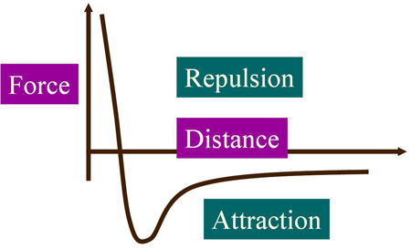
Figure 12.9. Probe-Surface interaction force vs distance. A qualitative representation
Note that in this representation, a positive force is repulsive and that a negative force is attractive. When the probe (i.e. tip) is far away, there is a slight attraction between the probe and the surface (Van der Wall forces), but when the distance becomes shorter, the net force is repulsive. In this region, even a slight change in the distance results in a large change in the interaction force. If the force can be monitored accurately, the distance between the tip and the surface can be measured accurately.
A photo of the AFM is given in figure 12.10 and the key components are illustrated in Figure 12.11. It consists of a very sharp ‘tip’, a laser, a photodiode system, xyz scanning system and a feedback control system.
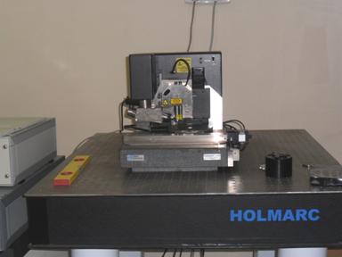
Figure. 12.10 A photo of AFM (Courtesy, Dept. Met. Metallurgy, IIT-Madras).
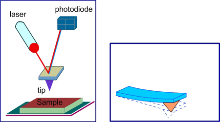
Figure 12.11 Schematic of the key components of AFM. 12.11b shows the schematic of the tip, which contains the probe mounted on a cantilever. The cantilever will easily bend even if there is a small force on the tip. The laser is reflected from the top surface of the cantilever, while the probe is attached to the bottom surface of the cantilever.
Description of the instrument: The instrument consists of a sharp tip, mounted on a cantilever. The cantilever acts like a very flexible spring. i.e. if there is a slight force on the tip, then cantilever will easily bend. The spring constant is in the range of less than1 N/m. The top surface of the cantilever is reflective. A laser is position to fall on the top surface, just above the probe, and reflect. The reflected light is detected using a four segment photodiode, as shown in Figure 12.11. The three components, viz. the laser, cantilever and the photodiode system are mounted in a rigid body. The detector position can be adjusted using the computer.
The sample (e.g. a wafer) will be kept on a stage which can be moved in x and y directions with nm level accuracy using piezoelectric system. The rigid body with the laser, cantilever and photodiode can be moved in Z direction accurately using another, independent piezoelectric system.
Operation: When the cantilever is in the ‘normal’ position, far away from any surface, the photo diode will be adjusted such that the beam will fall at the center of the photo diode segments. i.e. all the four segments will get equal amount of light. At this stage, the detector position will be fixed. Then the rigid body will be brought down so that the tip will be close to the surface. Once the probe comes close to the surface, the attractive forces will bend the tip towards the surface (as shown in Figure 12.12). This will cause the light to fall to different levels on the 4 segments of the photodiodes. When the tip comes closer to the surface, the repulsive forces will dominate and the cantilever will bend against the surface. The probe is said to be in contact mode. At this stage, the difference in light levels falling on the 4 segments will be converted to voltage and amplified. This can be called as ‘initial’ state. A particular voltage here corresponds to a particular probe-surface interaction force.
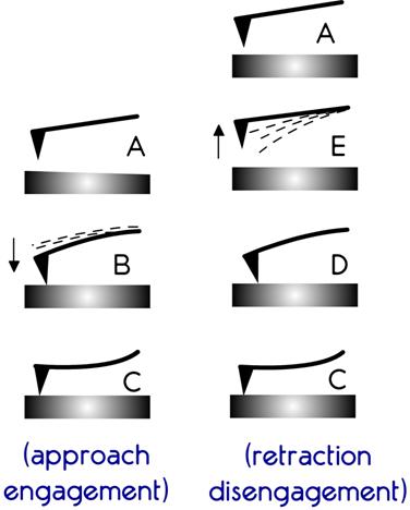
Figure 12.12 Illustration of cantilever movement with distance during approach and retraction
Now, using the X and Y piezo controllers, the sample surface will be moved. Depending on the surface topography, the distance between the probe and the surface will change. Hence the interaction force will also change. Thus, the cantilever will move, and the laser position on the detector will change. Subsequently, the measured force (i.e. voltage) will also change. Typically, a particular value of voltage will be set and a feedback controller will move the rigid body (Z piezoelectric controller) to move the probe up or down to bring the cantilever to the ‘initial’ state. i.e. the tip is constantly adjusted to maintain a set deflection and this maintains a constant height above the surface. The location in the x and y directions, and the distance moved in the z direction to bring the laser back to the ‘initial’ state will be recorded. The sample will be moved to the next ‘X’ location and the control loop will move the cantilever if necessary. The new X, Y and Z value will be recorded. At the end of one line (i.e. X direction), the sample will move one step in the Y direction, and the scanning in the X direction will continue. By recording the complete x,y,z information at all the places, a precise 3D map will be generated.
|