Then, P-type dopants are introduced in the PMOS regions.
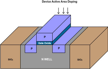
Fig 5.28 PMOS transistor formation. Step 7. Active area doping
Note that the gate region, as well as the source and drain are doped in one step. This also ensures that the gate comes exactly between the source and drain. If the source and drain were created first by doping those regions, before the poly silicon gate is created, then misalignments in the lithographic process can cause the gate to overlap with source or drain. However, in the process sequence explained above, the alignment comes naturally and this is called “self alignment” process. Then using photolithography and ion implantation, NMOS transistor regions are also made.
The top view of the PMOS transistor is given here. Note that source, drain and gate are extended and the connections (contacts) are made away from the transistor. This ensures that even if there is a slight misalignment during contact making process, the transistor will function correctly.
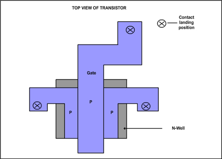
Fig 5.29 PMOS transistor. Top view, with contact landing positions
Once the doping is complete and the transistors are created, the surface of the source, drain and gate regions are treated with a metal. The connections to these source, drain and gate are made through metal contacts. From the contact region, the current has to flow through the source, channel and drain. To ensure that the resistance offered is small, cobalt is deposited on the top of the surface. Cobalt reacts with silicon (i.e. single crystal silicon in the source and drain region, and polycrystal gate region) and forms cobalt silicide. It does not react with silicon dioxide. In the next step, the unreacted cobalt is removed by wet chemical etching. This process is called silicidation. Thus, the semiconductor properties of silicon are relevant only below the surface, in the channel region. On the top, the current flows through the metal and the resistance offered is low.
After the silicidation process, silicon dioxide which also contains some boron and phosphorous (BPSG- boro phosphous silicate glass) is deposited on top of the wafer. Then through photo lithography and dry etching, holes are made in the BPSG. Tungsten is deposited by CVD and excess tungsten is removed by CMP. This results in the transistors with contacts which can be connected by Cu or Al interconnects in the subsequent steps in BEOL.
Transistor Isolation. Processes
In the previous section, we learnt that in the very beginning of the processing, transistor isolation is done. The transistors used to be isolated using a process called LOCal Oxidation of Silicon (LOCOS). However, in the last decade, a different process called Shallow Trench Isolation (STI) is used. The details of the STI process are given here. The reader may consider the older references for the details of LOCOS.
In the shallow trench isolation process, at first a thin layer of oxide is grown by thermal process and subsequently a thin layer of silicon nitride is deposited by CVD.
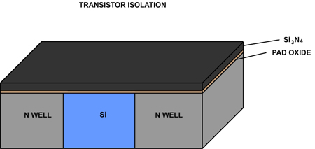
Fig 5.30 Isolation process. Step 1. Nitride deposition
In the next step, using photo lithography and etching, wherever electrical isolation is needed, a trench is made in silicon (i.e. the silicon nitride, silicon dioxide and then Si are removed by dry etching in those areas).
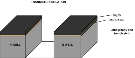
Fig 5.31 Isolation process. Step 1. Nitride deposition
Then silicon dioxide of sufficient thickness is deposited by CVD. Usually this is done using tetra ethyl oxy silane (TEOS) precursor and under high density plasma (HDP) conditions.
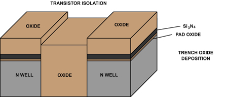
Fig 5.32 Isolation process. Step 2. Trench Oxide deposition
In the next step, the excess oxide is removed by chemical mechanical planarization. Here, care must be taken to ensure that only the oxide is removed and the nitride is not removed.
.jpg)
Fig 5.33 Isolation process. Step 3. Oxide CMP
Then the nitride is removed by wet etching using phosphoric acid.
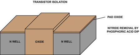
Fig 5.34 Isolation process. Step 5. Nitride removal
The slightly projecting oxide is removed by buffered hydrogen fluoride (BHF) etching. This ensures that a good quality insulator is present between the transistors.
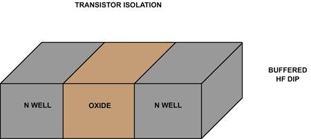
Fig 5.36 Isolation process. Step 5. Excess oxide removal
|