An important point to note is that a technology node or a process sequence for manufacturing a chip is usually denoted by the dimension or the size of the gate. If a technology node is called 35 nm or 65 nm then it means that the gate size the minimum size is 35 nm or 65 nm when it is planned in the layout. Many times the final size on the wafer may be different.
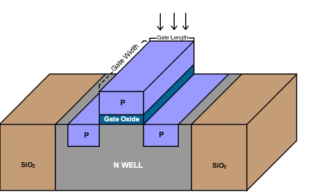
Fig 5.18 Schematic of a PMOS transistor in 3D
Gate length and width: Consider a transistor as seen from the top (shown in the 3D figure). The gate length and the gate width are marked as shown in the figure. Usually for a rectangle the longer size is called length and the shorter one is called width. However, for the transistor gate the shorter one is called length and the longer one is called width. Why? This is because when the transistor is switched on the electrons or the holes have to flow from the source to the drain. The distance or the length they travel is given by the size of the gate which is marked as length in the figure. So even though it is shorter it is called length because that decides how fast the transistor can operate. For example, when the transistor is switched on the gate voltage is adjusted and the current begins to flow. If the length as marked here is very long then it will take longer time for the transistor to become fully on. If it is small then the transistor can be switched on or off quickly. So, a smaller technology node allows the transistor to be switched on or switched off quickly. This means it allows for faster chip operation. It also means that within a given area if one can make small transistors they can fill the area with many more transistors which means the chip can be designed to have many functions.
I-V curves:
The voltage applied to the gate is called VG. When it exceeds a particular voltage the channel is formed and the transistor is switched on. This particular voltage is called threshold voltage or VT. The voltage difference between the source and the drain is called VDS . Normally the source will be grounded and the voltage will be applied to the drain. The difference VG-VT is called overdrive. A small change in VG will cause a large flow of current.
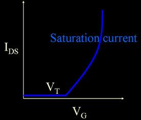
Fig 5.19 Schematic of drain-source current vs gate voltage
The threshold voltage VT depends on the following. It depends on the doping level of P. If the P type semiconductor has lot of holes, then large voltage has to be applied to the gate to fill in all the holes and give excess electrons. It also depends on the gate oxide thickness. If the oxide thickness is high, large voltage is applied to cause inversion and switch ON the transistor. The current flowing between the drain and source depends on the VG and it also depends on the drain to source voltage VDS as shown in the figure below.
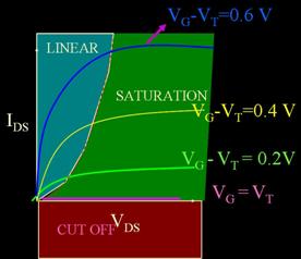
Fig 5. 20 Schematic of drain-source current vs drain-source voltage
When the gate voltage VG is less than or equal to the threshold voltage (VT), current does not flow for any value of VDS. When the gate voltage is more than the threshold voltage (e.g. VG-VT = 0.2 V), then the current IDS initially increases with the VDS. This region is called linear regime. After that, the IDS saturates to a value called IDSAT and an increase in VDS does not cause an increase in IDS. This is called saturation regime. If gate voltage is raised even higher, then the linear regime is broader, and the final saturation current IDSAT is more.
This can be understood with the following analogy. If we imagine that the source and the drain are two tanks filled with water and channel is a pipe connecting the two tanks and gate is a valve. When the height difference between the two tanks is zero no water will flow even when the valve is open. When one tank is raised above the other tank, then water can flow if the valve is open. So when source voltage is adjusted so that the electron can flow from source to drain in the NMOS. Then if the gate is opened, current will flow and if the gate is closed current will not flow. There are two ways to increase the flow, one to raise the level of tank that is to increase VDS, the other is to open the gate more. In the MOS transistors usually the gate is either fully open or fully closed. So this can be either full current will be flowing or no current will flow. These transistors are called digital transistors and these chips are called digital chips.
|