MOS Capacitor:
Before we learn about the MOSFET transistor we will see a simpler structure called MOS capacitor. The following image shows the schematic of MOS capacitor.
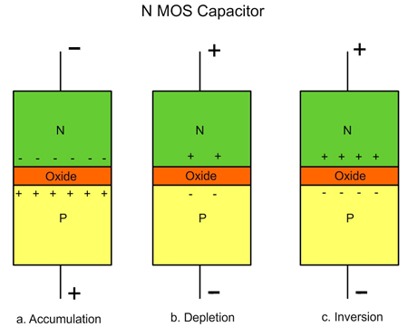
Fig 5.13 Schematic of a MOS capacitor under different regimes
This has N type material on the top, a thin oxide layer in the middle and a P type material at the bottom. The oxide here refers to silicon dioxide which is an insulator. When a P type material is connected to a positive terminal and N type is connected to a negative terminal of a battery, the electrons are withdrawn from the P type material and the excess electrons are given to the N type material. These accumulate near the oxide area. Now this is called accumulation stage. This is basically the structure of a capacitor where one side is positive and the other side is negative. In between these two sides there is a thin layer of insulator. Instead of these connections, if the positive and negative terminals are changed, we obtain what is known as depletion. Here electrons are withdrawn from the N type material and the excess electrons are supplied to the P type material. However before the connection P type material originally had excess of holes, N type materials originally had excess of electrons, because some of the electrons are withdrawn from the N type material because it is connected to the positive terminal. The amount of electrons available will be less. So this is depleted.
Similarly some of the holes on the P type will be filled because we are connecting negative terminal. Now on the P type material the number of holes is reduced or depleted. Hence this connection leads to depletion regime. What happens when we increase the voltage? When we apply a strong negative voltage to the P type and a strong positive voltage to the N type side, we obtain what is called inversion. On the N type side all the excess electrons are withdrawn and even more electrons are withdrawn leading to presence of holes. On the P side all the holes are filled and excess electrons are available leading to presence of additional electrons. Normally for N type electrons are majority carriers. Normally for P type holes are majority carriers. However because of the application of high voltage excess electrons are present in the P type now and excess holes are present in the N type now. This process is called inversion. Originally instead of N type silicon on the top, a metal was present and inversion was observed on the P silicon side. This structure was called Metal Oxide Semiconductor or MOS.
Later instead of metal, semiconductors are used but due to historic reasons the name metal oxide semiconductor is still used. With this background we can understand the operation of a transistor.
MOS transistor. Structure and operation:
The following schematic gives the structure of an NMOS transistor.
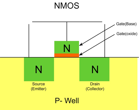
Fig 5.14 Schematic of a NMOS transistor
This is called NMOS because most of the materials here are N type semiconductors. It has the following structures source, gate, gate oxide and drain. The electrons are supplied to the source connection and the electrons are taken out or received at the drain side. The gate acts as a On -Off switch. It actually acts as a gate which allows the electrons to pass or it can close and stop the electron flow. Notice that below the gate oxide P type material is present. The question is : “Can we convert the P type material to appear as a N type material whenever we want?”. (If the entire block is made of N type material, then the electricity will flow from the source to drain without any problem). The answer is yes. The area below the gate can be made to appear as a N type material. Here, when we can say it can appear, we mean that electrons can be made as majority carriers in that area.
Consider the following schematic when the transistor is in Off condition.
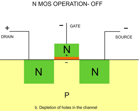
Fig 5.15 Schematic of a NMOS transistor under depletion mode
A negative voltage is given to the gate because it is given a negative voltage it accumulates electrons. All the electrons close to the oxide in the P area are repelled. Thus the P area has excess of positive charges or holes. Now current will not flow from the source to drain because the connection between the drain and the P type area is in reverse bias.
Consider the next schematic.
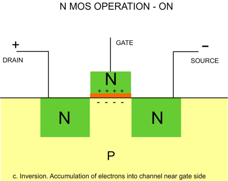
Fig 5.16 Schematic of a NMOS transistor under inversion mode
Here a positive voltage is given to the gate. This attracts the electrons near the oxide interface for the P type silicon area. If sufficient voltage is given, we saw that inversion will occur in MOS capacitor. The same phenomenon will occur here. The P type area will have excess of electrons. Thus it appears to be as N type silicon and hence current will flow. Thus by controlling the voltage applied for the gate, we can switch-on or switch-off the transistor whenever we want. In this transistor we change the voltage of the gate and influence the electric field and control the operation. Thus it is called field effect transistor or FET, because it uses MOS structure it is called MOSFET. This has N type material as source and drain, hence it is called NMOS. A similar structure where all the N is replaced by P and P is replaced by N will give a structure called PMOS, as shown below. The operation is very similar to the operation of NMOS.
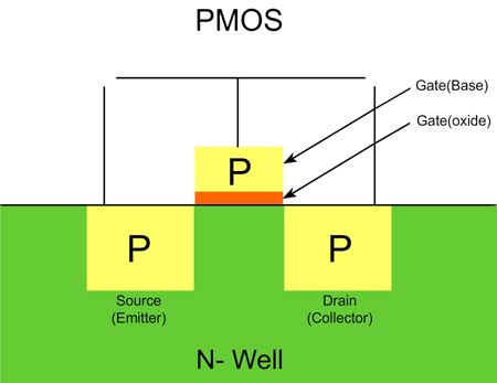 . .
Fig 5.17 Schematic of a PMOS transistor
In NMOS the source is connected to negative and the drain is connected to positive. In PMOS the source is connected to positive and the drain is connected to negative. Some of the terminologies used in the industry are given here. The current from drain to source is positive for NMOS and its called iDS for PMOS it is iDS which is negative. When the transistor is “on” the area below the gate oxide is called channel and we say that the channel is formed. When the transistor is switched off we say that the channel does not form.
|