Pinch off: When the transistor is operated in saturated regime, a phenomenon called “pinch off” occurs. Remember that for NMOS, the drain is positive while the source is negative. Since the drain is positive, when VDS is large (specifically, when VDS > (VG-VT)) all the electrons in the channel region near the drain will be pulled by the drain. Thus the channel practically disappears near the drain region. The onset of this phenomenon is called pinch off. Now, increasing the VDS will not affect the current and the current is mainly dependent on the gate voltage. Digital circuits are operated in the saturation current regime (i.e. pinch off mode).
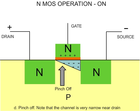
Fig 5.21 Schematic of a NMOS transistor with pinch off
When the VDS is large, the electrons from the source (for NMOS) are accelerated in the channel and arrive at the drain with high velocities and hence high kinetic energies. These are equivalent to electrons at high temperatures. These can cause degradation of the transistor or instability. This phenomenon is called hot carrier effect. For PMOS transistor, the carriers are holes. One of the problems that can arise due to hot carrier effect is that the electrons may go through the gate oxide into the gate. Thus, the gate oxide will be degraded and the threshold voltage will change.
To minimize the hot carrier effect, the drain near the channel can be doped less compared to the main drain area. This is called lightly doped drain (LDD). To minimize the process complications, both source and drain are doped lightly near the channel region. A schematic of transistor with LDD is given below.
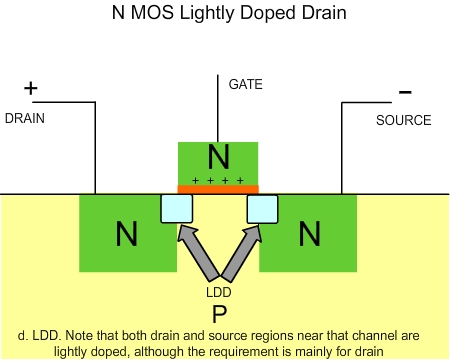
Fig 5.22 Schematic of a NMOS transistor with lightly doped drain
Transistor formation. Processes:
We have learnt about the structure and operation of a MOS transistor. In this section, we will learn about the sequence of processes needed to create a MOS transistor. The MOS transistors are always created in a “Well” region. A PMOS transistor is made in an N-doped region, called “N-Well” region. Similarly, an NMOS transistor is made in a “P-type” region called “P-Well”. This ensures that the leakage between two transistors, through the bottom side, is low. This is because of the reverse bias between the transistor areas and the well region.
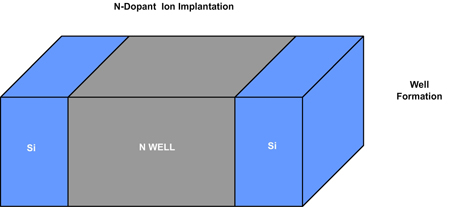
Fig 5.23 PMOS transistor formation. Step 1. Well formation
The first step in the formation of transistor is the “Well” creation. Consider a region where a PMOS transistor must be created. A layer of silicon dioxide is first formed on the wafer and using lithography and dry etching, a window is opened. Next, N-dopants are introduced by ion implantation in the N-Well regions. Similar set of operations are conducted to create P-Well regions.
Once the well is created, an insulated area is created between the transistors. This is called transistor isolation and it will be discussed in the next section in detail. Thus, the insulation is made even before the transistors are made.
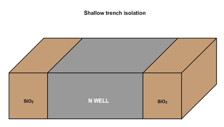
Fig 5.24 PMOS transistor formation. Step 2. Isolation
Next, a thin layer of oxide is formed on the surface, by thermal oxidation.
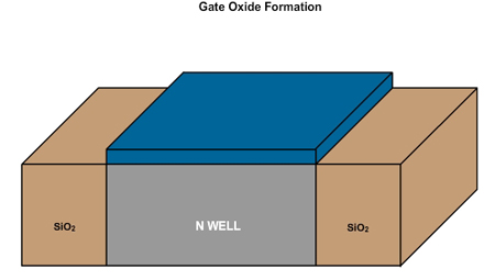
Fig 5.25 PMOS transistor formation. Step 3. Gate oxide formation
Then, a layer of poly silicon is deposited by CVD.
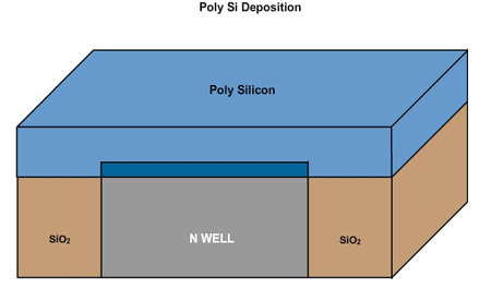
Fig 5.26 PMOS transistor formation. Step 4. Poly deposition
Next, using lithography and etching, unwanted poly silicon and oxide layers are removed. After this step, the structures will appear as given in the schematic below.
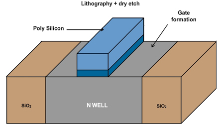
Fig 5.27 PMOS transistor formation. Step 6. Gate formation
|