In this chapter we will learn the basics of semiconductor electrical properties. We will also learn about the structure and operation of the semiconductor devices. Only a limited amount of details will be discussed here and for further details books on Solid State Physics and Basis Electronic Engineering can be referred. The following topics will be considered. 1. Band structure, 2. Diode, 3. MOS device capacitor 4. MOS transistor structure and operation and 5. Transistor formation and 6. Transistor isolation
Electronic band structure:
First we will consider the band structure and the band gaps of conductor’s insulators and semiconductors. In general a material can be classified as electrical conductor or insulator or semiconductor. Normally when electricity is passed through a semiconductor it offers significance resistance, but the insulator will not allow the current to pass through it. A conductor will allow the current to pass through it easily. The following figure gives the approximate conductivity and various materials which are grouped based on the conductivity.

Fig 5.1 Various materials grouped by their electrical conductivity
Metals are materials with very high conductivity. Some examples are copper, silver, aluminum etc. Materials such as germanium or silicon are semiconductors. Materials such as phosphorous, glass and Teflon are insulators. Please note that the material boron and material phosphorous are highlighted, they are insulators. They play a significant role in transistor operation. We will see the details at the later stage. In metals the electricity is conducted by electrons; in semiconductors there are two charge carriers one is electron; the other is hole.
When an electron is removed from a material the vacancy created is called hole. It can be thought of as a positive charge. In a pure semiconductor such as silicon, the number of electrons available for electricity conduction and the number of holes will be equal. When the temperature is increased there will be more electrons and more holes and hence the conductivity will be higher. The electrons in an atom can be present only at certain energy levels. For example, the quantum mechanics Schrodinger’s equation is usually solved for hydrogen atom and various allowed energy levels can be calculated. However the solution that is normally presented in the classroom is for a single hydrogen atom.
When the solution is obtained for other materials and particularly for many atoms together, the allowed energy levels will form bands. When two identical atoms come together the solution of Schrodinger equation is different from one atom alone. Pauli’s exclusion principle which applies for electrons says that two electrons cannot be at the same energy level. Hence 2 energy level appears. We can say that the one energy level obtained for the hydrogen atoms electron is now split into two. When many atoms come together and they are in close proximity, the energy level solution is split into many levels. When they are very close together they appear to be a band. This is shown in schematic below.

Fig. 5.2. Schematic of electronic structure of a single atom and multiple atoms
The size of the band depends on the spacing between the atoms. This is shown in schematic-2.

Fig 5.3 Schematic of the variation of energy level with distance between the atoms
Now what is the difference between metals which are good conductors and insulators and semiconductors? When we look into the allowed energy bands of the material, the structure is different for metals. All the lower energy levels are filled and at the highest energy level the energy levels of the filled bands overlap with the energy levels of the empty bands.

Fig 5.4 Schematic of the energy levels in a metal
When the electrons are filling from the bottom, the top most occupied level is called valance band. After that empty levels start. The energy band which is just above the valance band that is the bottom most empty level is called conduction band. When both of them overlap it means the electron in the valance band can go to the conduction band with very little energy.
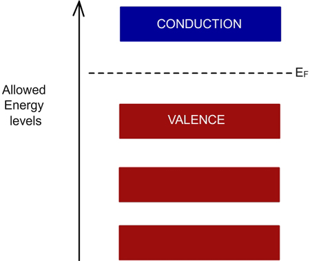
Fig 5.5 Schematic of the energy levels with valence and conduction bands marked
Only the electron in the conduction band can participate in electrical conduction. The band structure for an insulator is given below.
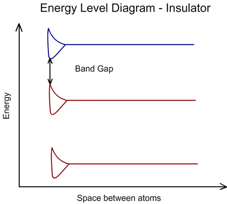
Fig 5.6 Schematic of the energy levels in an insulator
Here the valance band and the conduction band are separated by a significant amount of energy. The electron at the valance band needs energy to go to conduction band. Hence normally this material will not conduct electricity. The distance between these two bands is called band gap. When the band gap is high, the material is an insulator. Semiconductors are similar to an insulator which means the valance band and conduction band do not overlap. However the band gap is small. Even at room temperature, some of the electrons will have some energy to move from valance band to the conduction band and conduct electricity.
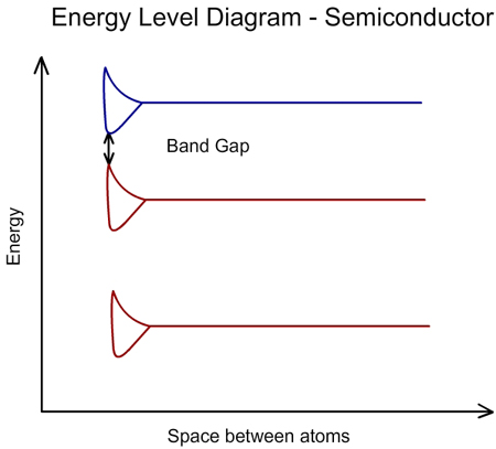
Fig 5.7 Schematic of the energy levels in a semiconductor
|