Scanning electron microscopy
A scanning electron microscope is usually equipped with the detectors for secondary electrons and backscattered electrons (refer to figure 18.3). An SEM can produce images up to a resolution of ~2.5 nm. Some of the applications of SEM are:
Surface morphology: Imaging of the specimen at nanometer scale resolution is perhaps the most-straightforward application of SEM. Biological specimens are dried and coated with a conducting material as discussed in lecture 18.
Compositional analysis: Backscattering of electrons depends on the atomic number of the material. Backscattered electrons reveal the differences in the composition of a material. The regions with high atomic mass elements scatter more electrons thereby giving a brighter image. This kind of analysis allows detection of the contaminants in a specimen, if any.
Energy dispersive X-ray spectroscopy (EDS/EDX/EDXS): EDXS is one of the several analytical electron microscopic methods. The primary electron beam causes excitation of the atoms in the specimen by ejecting electrons form their inner shells. The hole thus created is filled by an electron from the outer high energy shells. The excess energy is emitted as the X-rays that are characteristic of the element; determination of their energies allows identification of the elements in the specimen (Figure 20.2).
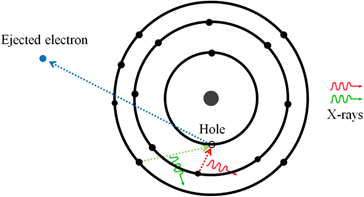
Figure 20.2 A diagrammatic representation of X-rays production by an atom.
Transmission and scanning transmission electron microscopy
Transmission electron microscopy has become a routine method for studying the biological specimens. A resolution of <0.5 nm is easily achieved as compared to ~2.5 nm resolution limit of SEM. Let us look at the various applications of TEM:
Bright-field and dark-field microscopic imaging: Unless mentioned otherwise, TEM images usually are bright-field images. Thicker and electron-rich regions in the specimen produce darker regions in the image. Owing to their sub-micrometer/nanometer dimensions, many of the cellular components are not observed by light microscopy. High resolution TEM can reveal the ultrastructural details of these components. Like light microscopy, TEM can operate in dark-field mode too. An aperture can be adjusted to reject the undiffracted electron beam; the diffracted electrons generate an image against a dark background.
Electron diffraction: The crystalline regions in the specimen diffract the incident electrons. The diffraction pattern generated provides information about the lattice parameters of the crystalline regions.
Energy dispersive X-ray spectroscopy (EDS/EDX/EDXS): Analytical transmission electron microscopes usually come with several detectors such as detectors for secondary electrons, backscattered electrons, and X-rays . If a TEM is used in scanning mode (Scanning TEM/STEM), a compositional map can be obtained for the specimen.