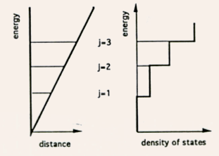
Fig.4.22 Energy levels (bottoms of subbands) and density of states for
a triangular quantum well structure (j = 1, 2, …, correspond to the
different subbands).
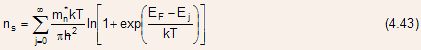
- After evaluating this integral and adding the contribution from all subbands, one obtains
- The quantized energy levels for the subbands can be found using a
numerical self-consistent solution of the
 dinger and Poisson's equations.
- However, an excellent approximation for the exact solution can be
found by assuming a linear potential profile (i.e., constant effective
field Feff) in the semiconductor and close to
the semiconductor-insulator interface.
- In this case, the energy levels are given by
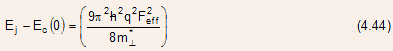
where ![]() is the
effective mass for electron motion perpendicular to the (100) surface,
and Ec(0) is the minimum conduction band energy
at the Si-SiO2
interface.
is the
effective mass for electron motion perpendicular to the (100) surface,
and Ec(0) is the minimum conduction band energy
at the Si-SiO2
interface.
- The effective field Feff is expressed through
the surface field FS and the bulk field FB.
- For electrons, the relationship linking Feff,
FB, and FS, giving the best
fit to the self-consistent solution of
dinger and Poisson's equation is given by
 and Feff = (FS + FB)/2,
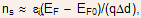
where ns is the interface electron sheet density, and qnB
(= qNAddep(av)) is the sheet
density of depletion charge.
and Feff = (FS + FB)/2,
where ns is the interface electron sheet density, and qnB
(= qNAddep(av)) is the sheet
density of depletion charge.
- Similarly, for holes, FS = q(ps
+
 where
ps is the interface hole sheet density, and qpB
(= qNDddep(av)) is the sheet
density of depletion charge.
where
ps is the interface hole sheet density, and qpB
(= qNDddep(av)) is the sheet
density of depletion charge.
- In reality, it has been found that a slightly different form of the
effective field Feff1 = (FS
+ 2FB)/3 gives a better fit to the measured data.
- Solving these equations iteratively, one can obtain the relation between ns and the Fermi level [EF Ec(0)].
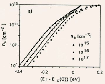
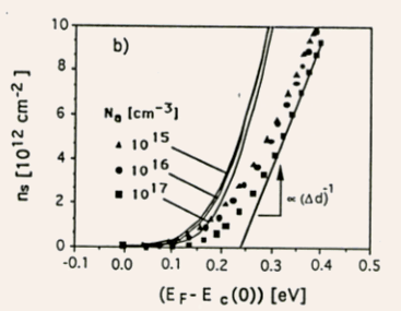
Fig.4.23 Comparison of the interface carrier density versus EF
Ec(0) characteristics for different substrate doping
densities in (a) semilog plot and (b) linear plot. Symbols: calculations
based on a 2DEG formulation, solid lines: charge sheet model, straight
line in b): linear approximation to 2DEG formulation, the slope gives
![]()
- In the calculation, it can be assumed that the maximum value of nB is given by
![]()
- In the subthreshold region, the calculation agrees reasonably well with the classical charge sheet model (CCSM) given by Brews:
![]()
especially at low levels of substrate doping.
- The difference between the curves at high substrate doping levels
is caused by the fact that the large bulk field quantizes the energy
levels even in the subthreshold region.
- However, at strong inversion, the difference between the charge sheet
model and the 2DEG formulation is large.
- As can be seen from Fig.4.23, the dependence of ns
on EF in the above threshold regime can be approximated
by a straight line:
 where EF0 is the intercept of this linear approximation
with ns = 0.
where EF0 is the intercept of this linear approximation
with ns = 0.
- This approximation means that a fraction of the applied voltage, equal
to
 is accommodated
by a shift in the Fermi level with respect to the bottom of the conduction
band.
is accommodated
by a shift in the Fermi level with respect to the bottom of the conduction
band.
- The shift in the Fermi level with respect to the bottom of the conduction
band changes the above-threshold capacitance from to
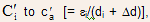 where the parameter
  can be interpreted as a correction to the insulator thickness.
- From the straight-line approximation in Fig.4.23b),
 is obtained, which is much smaller than that of
- This difference is caused by
- a much larger effective mass in the conduction band in Si,
which makes quantum effects much less pronounced, and
- the large difference in the dielectric constants between the insulator and the semiconductor for the MOS system.
- a much larger effective mass in the conduction band in Si,
which makes quantum effects much less pronounced, and
Practice Problems
4.1 Clearly draw the band diagrams for an ideal MOS structure ![]() and no oxide charge) on n-type Si for i) accumulation,
ii) depletion, and iii) inversion. If the oxide thickness tox
= 40 nm and VG = 1 V, determine the magnitude
and no oxide charge) on n-type Si for i) accumulation,
ii) depletion, and iii) inversion. If the oxide thickness tox
= 40 nm and VG = 1 V, determine the magnitude ![]() and sign of the charge density in the semiconductor. What is the status
of the surface?
and sign of the charge density in the semiconductor. What is the status
of the surface?
4.2 Show that for an MOS structure on p-type Si,
the electron and hole concentrations as functions of position are given
by ![]() where
n0 and p0 are the equilibrium
electron and hole concentrations respectively, and
where
n0 and p0 are the equilibrium
electron and hole concentrations respectively, and ![]() is defined by
is defined by ![]() = [Ei(bulk) Ei(x)]/q.
= [Ei(bulk) Ei(x)]/q.
4.3 Continuing with the derivation given in Section 4.2, show that the
electric field E in the semiconductor in an MIS capacitor can be given
by ![]() where
all the notations carry their usual meanings.
where
all the notations carry their usual meanings.
4.4 Sketch the electric field and voltage distribution in an MOS structure
at the threshold gate voltage. Data:![]() substrate voltage = 0, and VFB = 0. Compute the
threshold voltage VTH from the voltage distribution.
substrate voltage = 0, and VFB = 0. Compute the
threshold voltage VTH from the voltage distribution.
4.5 Calculate and plot the semiconductor surface charge ![]() per unit area for an MIS structure as a function of the surface potential
per unit area for an MIS structure as a function of the surface potential
![]()
4.6 Starting from Eqn.(4.16), show that at flatband (i.e., when Vs
= 0), the flatband capacitance per unit area ![]() Hence, compute its magnitudes for substrate dopings of
Hence, compute its magnitudes for substrate dopings of ![]()
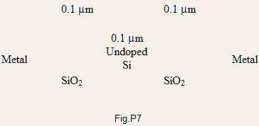
4.7 Consider the energy band diagram of a metal-SiO2-Si-SiO2-metal
structure as shown in Fig.P7. Assume symmetric bands with ![]()
(a) What is the flatband voltage for this structure?
(b) Sketch the band diagram of the structure when the left metal plat
is at 2 V and the right metal plate is grounded. Assume ![]() What
is the strength of the electric field in Si? What
are the positions of the Imrefs in Si? In the band
diagram, all the appropriate voltage levels must be specified. Neglect
induced charges in Si.
What
is the strength of the electric field in Si? What
are the positions of the Imrefs in Si? In the band
diagram, all the appropriate voltage levels must be specified. Neglect
induced charges in Si.
4.8 (a) Find the voltage VFB required to reduce
to zero the negative charge induced at the semiconductor surface by a
sheet of positive charge ![]() located
located ![]() below
the metal.
below
the metal.
(b) In the case of an arbitrary distribution of charge ![]() in the oxide, show that
in the oxide, show that
![]()
where ![]() =
oxide capacitance per unit area =
=
oxide capacitance per unit area = ![]() where d = oxide thickness.
where d = oxide thickness.
4.9 Charge density of ![]() is distributed in the oxide (d = 40 nm) in a Si
MOS capacitor. Assume
is distributed in the oxide (d = 40 nm) in a Si
MOS capacitor. Assume ![]() Find
the flatband voltage required to be applied at the gate to compensate
these charges if: i) the charges are uniformly distributed in the oxide,
ii) the charge distribution is linear with the peak at the metal-SiO2
interface and zero at the Si-SiO2
interface, and iii) same as ii) but now with the peak at the Si-SiO2
interface and zero at the metal-SiO2
interface. Physically justify the answers.
Find
the flatband voltage required to be applied at the gate to compensate
these charges if: i) the charges are uniformly distributed in the oxide,
ii) the charge distribution is linear with the peak at the metal-SiO2
interface and zero at the Si-SiO2
interface, and iii) same as ii) but now with the peak at the Si-SiO2
interface and zero at the metal-SiO2
interface. Physically justify the answers.
4.10 An Al-gate ![]() where m is the Al work function to vacuum) MOS structure is made on p-type
where m is the Al work function to vacuum) MOS structure is made on p-type
![]() % where is
electron affinity for Si) substrate. The SiO2
thickness d = 50 nm, and the effective oxide interface charge
% where is
electron affinity for Si) substrate. The SiO2
thickness d = 50 nm, and the effective oxide interface charge ![]()
![]() Find Wmax, VFB, and VTH.
Sketch the C-V curve for this device giving all relevant details.
Find Wmax, VFB, and VTH.
Sketch the C-V curve for this device giving all relevant details.
4.11 Find VTH for an MOS structure in Si
with p-type substrate ![]()
![]() and d = 80 nm. Repeat for n-substrate
and d = 80 nm. Repeat for n-substrate ![]() with the same parameters (note: the new
with the same parameters (note: the new ![]() can be calculated from the change in EF).
can be calculated from the change in EF).
4.12. Calculate and plot the maximum width of the depletion region for
an ideal (i.e., VFB = 0) MIS capacitor on p-type
Si with ![]() as a function of the substrate bias Vsub for -2
V < Vsub < 0.1 V. Assume that the voltage
difference between the inversion layer at the interface and the gate contact
is maintained constant when the substrate potential is changed (charge
screening), so that the substrate voltage reverse biases the inversion
layer/p-type substrate junction. Also, calculate the threshold voltage
VT, and the capacitance of the structure at low
and high frequencies for V >> VT for Vsub
= 0. Data: ni =
as a function of the substrate bias Vsub for -2
V < Vsub < 0.1 V. Assume that the voltage
difference between the inversion layer at the interface and the gate contact
is maintained constant when the substrate potential is changed (charge
screening), so that the substrate voltage reverse biases the inversion
layer/p-type substrate junction. Also, calculate the threshold voltage
VT, and the capacitance of the structure at low
and high frequencies for V >> VT for Vsub
= 0. Data: ni = ![]()
4.13 Calculate and plot the surface potential ![]() as a function of the gate voltage VG in depletion
and inversion for a two-terminal MIS structure. Identify the weak inversion,
moderate inversion, and the strong inversion regions in the plot (as per
Tsividis). Can the plot be really linearized in subthreshold? Determine
an effective value of
as a function of the gate voltage VG in depletion
and inversion for a two-terminal MIS structure. Identify the weak inversion,
moderate inversion, and the strong inversion regions in the plot (as per
Tsividis). Can the plot be really linearized in subthreshold? Determine
an effective value of ![]() in subthreshold
from the plot.
in subthreshold
from the plot.
4.14 Calculate and plot the gate-to-substrate capacitance Cmis
as a function of the gate voltage VG for a two-terminal
MIS structure with area = ![]() The plot should show all the regions of operation (i.e., accumulation,
depletion, weak inversion, and strong inversion). Mark Cso
in the plot, with the magnitude shown. (Note: the externally measured
capacitance includes the oxide capacitance).
The plot should show all the regions of operation (i.e., accumulation,
depletion, weak inversion, and strong inversion). Mark Cso
in the plot, with the magnitude shown. (Note: the externally measured
capacitance includes the oxide capacitance).
4.15 Calculate and plot the temperature dependence of the surface charge
per unit area ![]() for the surface potential i)
for the surface potential i) ![]() in the temperature range between 150 K and 450 K. Data: effective densities
of states in conduction and valence bands
in the temperature range between 150 K and 450 K. Data: effective densities
of states in conduction and valence bands ![]() and
and ![]() respectively
at 300 K (with both of them having a
respectively
at 300 K (with both of them having a ![]() dependence), and the energy gap Eg = 1.12 eV (the variation of the energy
gap with temperature may be neglected).
dependence), and the energy gap Eg = 1.12 eV (the variation of the energy
gap with temperature may be neglected).
4.16 From the equivalent circuit for an MIS structure, determine the
expression for the impedance across its two terminals as a function of
frequency. Hence, calculate and plot the effective capacitance
of the structure as a function of the gate voltage VG
(varying from -5 V to +5 V) for frequencies of ![]()
![]()
4.17 As a practice problem, draw any arbitrary C-V curve of your choice, and following the parameter extraction algorithm discussed in Section 4.4.1, obtain the i) oxide thickness, ii) threshold voltage, iii) substrate doping, iv) flatband capacitance, v) flatband voltage, and vi) fixed oxide charges.
4.18 The C-V curve of a two-terminal MIS structure ![]() shows a shift of 10 mV in the flatband voltage after a bias-temperature
stress test. If the flatband voltage before the stress test is -1 V, and
the surface state density is
shows a shift of 10 mV in the flatband voltage after a bias-temperature
stress test. If the flatband voltage before the stress test is -1 V, and
the surface state density is ![]() determine the oxide fixed charges.
determine the oxide fixed charges.
4.19 Derive Eqn.(4.40).
4.20 Derive Eqn.(4.43).
4.21 (a) Compute and plot the surface electron concentration ns
as a function of [EF - EC(0)]
under the 2DEG approximation for ![]()
(b) Repeat part (a) under the 3D approximation (i.e., the 3D charge sheet
model as given by Brews).
Data: ![]() (Note:
the constant energy surface for Si consists of six
ellipsoids of revolution, and ml (
(Note:
the constant energy surface for Si consists of six
ellipsoids of revolution, and ml (![]() ) and mt (
) and mt (![]() ) represents the lateral and transverse effective mass respectively. For
{100} direction four of these ellipsoids will lye on the surface and two
ellipsoids will be perpendicular. Refer to Problem 22 also.)
) represents the lateral and transverse effective mass respectively. For
{100} direction four of these ellipsoids will lye on the surface and two
ellipsoids will be perpendicular. Refer to Problem 22 also.)
4.22 In the classical limit, the separation of the energy subbands in a 2D electron gas is small compared to the thermal energy kT. In this case, the sheet density of the 2D electron gas is given by the classical charge sheet model, given by Eqn.(4.46), which is derived using a conventional 3D electron gas approach. Show that in this limit (i.e., Ej Ej 1 << kT), the equation
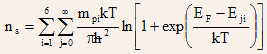
reduces to Eqn.(4.46). In the above equation, mpi
is the parallel effective mass for the valley i, and Eji
is the energy level of the jth subband in valley i.
Note: the effective mass mpi is mt
for two valleys, and ![]() for four valleys, where mt and ml
is the transverse and lateral effective mass respectively.
for four valleys, where mt and ml
is the transverse and lateral effective mass respectively.
| 4 |