EXAMPLE 4.3: Draw the low- and high-frequency C-V characteristics, clearly showing all the relevant points, including the flatband capacitance, for a two-terminal MIS structure having 30 nm thick oxide and substrate doping of 1015 cm 3 (p-type). Assume VFB = 1 V.
SOLUTION: The oxide capacitance per unit area
![]()
The bulk potential
![]() = (kT/q)
ln(NA/ni) = 0.026 ln[1015/(1.5
1010)] = 0.29 V
= (kT/q)
ln(NA/ni) = 0.026 ln[1015/(1.5
1010)] = 0.29 V
The threshold voltage
![]()
![]()
The maximum width of the depletion region
The semiconductor capacitance per unit area at threshold
Therefore, the total capacitance per unit area at threshold
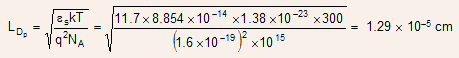
The Debye length
The flatband capacitance per unit area
![]()
-
The capacitance Csc becomes dominant in the strong inversion region, when the surface electron concentration is appreciable, since the band bending is largest at the surface.
-
Note: the electrons, which create the inversion region near the surface, are actually generated in the bulk due to thermal EHP generation.
-
Due to the electric field near the surface (recall that electric field points uphill in the band diagram), the electron and hole of the generated EHP are separated; the electron moves towards the surface and the hole moves towards the bulk => thus the rate of electron build-up near the surface proceeds at a rate limited by the rate of thermal EHP generation.
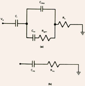
Fig.4.9 (a) The exact high-frequency equivalent circuit of a two-terminal
MIS structure, and (b) its simplified equivalent.
-
Two new components in the equivalent circuit:
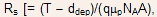 where
T is the thickness of the semiconductor layer, and
where
T is the thickness of the semiconductor layer, and  is
the hole mobility] is the resistance of the quasi-neutral p-region,
and
is
the hole mobility] is the resistance of the quasi-neutral p-region,
and
- Rgen (= dVs/dIgen)
is a differential resistance, which is a characteristic of the EHP
generation process.
-
Igen is the generation current, given by
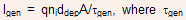 is
an effective generation time constant.
is
an effective generation time constant.
-
Thus, for gate voltages smaller than the threshold voltage VT,
![]()
-
In the small-signal equivalent circuit, the parameters Ceq and Req are given by
![]()
where ![]()
and
-
Note: both Ceq and Req are frequency dependent: in the limiting case of
 +
Cdep, and in the other limiting case of
+
Cdep, and in the other limiting case of
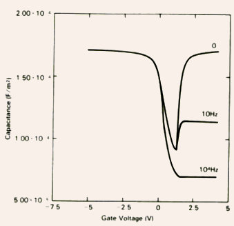
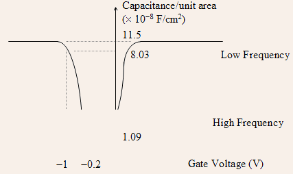
Fig.4.10 The C-V characteristics for a two-terminal MIS structure at
different frequencies.
4.4.1 Extraction of Parameters from the C-V Characteristic
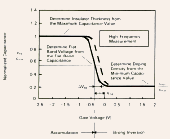
Fig.4.11 Parameter extraction from the C-V characteristic for a two-terminal
MIS structure. The parallel shift in the characteristic after the bias-temperature
stress test (described later) is also shown.
-
The maximum measured capacitance Cmax in the accumulation region gives the dielectric thickness

- The minimum measured capacitance Cmin at high
frequency gives the doping concentration (assumed uniform) in the substrate.
Steps:
-
First, determine the depletion capacitance Cdep in the strong inversion region from 1/Cdep = 1/Cmin 1/Cmax.
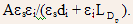
- Then, obtain the depletion region thickness from
- And, finally, calculate the doping concentration from the following
two equations:

- These two equations need to be solved by iteration: first choose
a suitable value for
 (say, 0.3 V), obtain NA, recalculate ,
obtain another fine tuned value of NA, and repeat
the process until the desired accuracy is achieved.
(say, 0.3 V), obtain NA, recalculate ,
obtain another fine tuned value of NA, and repeat
the process until the desired accuracy is achieved.
- It also gives the information about the flatband voltage VFB.
Steps:
- The device capacitance CFB under flatband condition
can be given by CFB = CiCs0/(Ci
+ Cs0) =
- Thus,
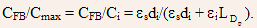
- From a knowledge of di and NA, CFB/Cmax can be obtained, and the intercept can be found on the C-V curve to yield VFB.
- The device capacitance CFB under flatband condition
can be given by CFB = CiCs0/(Ci
+ Cs0) =
4.5 Non-ideality in an MIS Structure: Oxide Charges
- In most of the commercially available MOS capacitors and MOSFETs,
silicon (Si) is used as the semiconductor and
silicon dioxide (SiO2) is
used as the insulator.
- Si being a crystalline material and SiO2 being an amorphous material, there is a sudden discontinuity in the lattice structure at the Si-SiO2 interface.
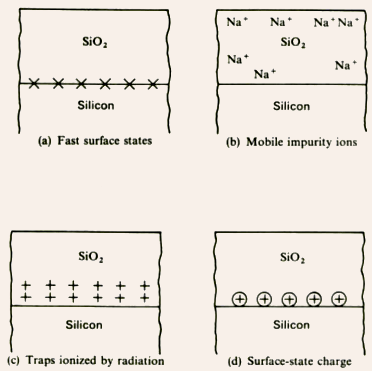
Fig.4.12 Different types of charges in the Si-SiO2
interface and in the SiO2 layer.
- This interface has attracted considerable interest over the last
few decades, and significant studies have been made on this structure,
however, a detailed understanding of many of its features is still lacking.
- The interface and the oxide contains various types of charges, which can be broadly categorized into the following:
- Charges due to fast surface states (or interface trapped charges)
 located at the interface.
- Charges due to mobile impurity ions
 located in SiO2.
 - Charges due to traps ionized by radiation
 within
SiO2.
within
SiO2.
- Fixed surface state charges
 located at the interface.
4.5.1 Fast Surface States
- These are also referred to as Tamm and Shockley states, after their
inventors.
- These are created at the interface due to the sudden termination of
the crystal periodicity, since all the bonds of the atoms at the surface
are not fulfilled these unfulfilled bonds are referred to as the dangling
bonds.
- Obviously, the density of these states is a function of the crystal
orientation (since (100) planes have lower atom density than (111) planes,
MOSFETs are universally fabricated on (100) oriented Si).
- Roughly, one fast surface state is assigned for every surface atom,
resulting in a density

- Proper cleaving of the surface and consequent heat treatment with
H2 drastically reduces the density of these states
to
 or so,
since H2 compensates some of these dangling bond
by the formation of SiH.
or so,
since H2 compensates some of these dangling bond
by the formation of SiH.
4