![]()
reaches its maximum value for
![]()
- Hence, the following sheet inversion charge density at threshold is obtained:
![]()
and the value for the unified capacitance per unit area at threshold becomes
![]()
- Here,
 is
the maximum value of
is
the maximum value of 
- Equation (4.33) serves as the basis for a very convenient and straightforward technique for determining the threshold voltage from experimental data.
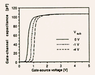
Fig.4.17 Measured gate-channel capacitance as a function of gate-source
voltage for an n-channel MOSFET for different values of substrate bias.
- From the experimentally determined gate-channel capacitance, the inversion carrier sheet density can be calculated as
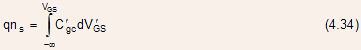
- According to UCCM, this should agree with Eq.(4.29), which can be written as
![]()
- Hence, from a plot of
 versus
 and a can
be found.
and a can
be found.
- The slope of this plot gives
 , while the intercept with
  yields a.
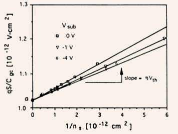
Fig.4.18 Inverse gate-channel capacitance plotted as a function of the
inverse mobile sheet charge density (data obtained from Fig.4.17).
Fig.4.19 Measured dependence of ![]() (curves to the left) and -1 V (curves to the right). The threshold voltages
determined by the two methods are also indicated.
(curves to the left) and -1 V (curves to the right). The threshold voltages
determined by the two methods are also indicated.
- The values of
 obtained
from the slopes in Fig.4.18 agree very well with those determined directly
from the subthreshold I-V characteristics, and the value of di calculated
from a is in excellent agreement with that measured by ellipsometry.
obtained
from the slopes in Fig.4.18 agree very well with those determined directly
from the subthreshold I-V characteristics, and the value of di calculated
from a is in excellent agreement with that measured by ellipsometry.
- In Fig.4.19, the value of VGS corresponding
to the peak value of
 should
coincide with the value of VGS at which the gate-channel
capacitance has dropped to one-third of its maximum value.
should
coincide with the value of VGS at which the gate-channel
capacitance has dropped to one-third of its maximum value.
- In Fig.4.20, the agreement between the measured and the calculated data is excellent for the entire range of gate bias.
Fig.4.20 Measured (solid lines) and calculated (UCCM, symbols) ns versus VGS characteristics for different values of Vsub in (a) semilog scale and (b) linear scale. In (b), the results obtained from the simple charge control model (SCCM) are also shown.
- The deviation in the measured curves found in the deep subthreshold
region is due to two reasons: one is the C-V measurement error, and
the other is the leakage current, which dominates deep subthreshold
operation.
- At deep subthreshold, the channel offers a large series resistance
compared with the reactance of the capacitance.
4.7.1.1 Analytical Unified MIS Capacitance Model
- Note: the UCCM does not have an exact analytical solution for the
inversion charge in terms of the applied voltage even though an accurate
approximate solution can be obtained.
- Above threshold, the sheet density of carriers in the inversion layer can be given as
![]()
- Below threshold, the electron sheet density in the channel can be written as
![]()
- From Eq.(4.37), the following expression is obtained for the subthreshold differential channel capacitance per unit area
![]()
- An approximate, unified expression for the effective differential
metal-channel capacitance per unit area
 is
obtained by representing it as a series connection of the above threshold
and the subthreshold capacitances, i.e.,
is
obtained by representing it as a series connection of the above threshold
and the subthreshold capacitances, i.e.,
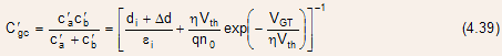
- Hence, the unified carrier sheet charge density becomes
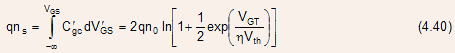
- Equation (4.40) is similar to an interpolation formula, and calculations show that it is in excellent agreement with UCCM.
4.8 Quantum Theory of the Two Dimensional Electron Gas (2DEG)
- Classically, the electrons induced at the semiconductor-insulator
interface of an MIS capacitor form a classical electron gas and behave
essentially in the same way as electrons in a bulk semiconductor.
- This assumption is only correct if the thickness of the inversion
layer is much larger than the deBroglie wavelength
 for electrons.
- For the classical electron gas, this thickness d can be estimated
as
 where
Fs is the surface electric field, and using Gauss'
law, this field can be approximated as
where
Fs is the surface electric field, and using Gauss'
law, this field can be approximated as 

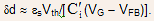
- In this estimate, the condition of continuity of electric displacement
across the semiconductor-insulator interface is used, and it is assumed
that almost all of the applied voltage drops across the insulator.
- Hence,
- In modern day MOSFETs, di can be well below
100 , and
 may become smaller than the deBroglie wavelength, e.g., for di = 100


- In this case, the quantization of the energy levels in the potential
well at the semiconductor-insulator interface in the direction perpendicular
to the interface must be taken into account.
- Once quantization of energy levels take place, then the dispersion (E-k) relation in the direction parallel to the interface is given by:
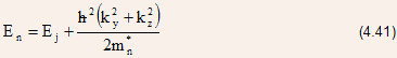
where En is the electron energy, Ej is the energy level of the jth subband, and ky and kz are the wave vector components parallel to the interface.
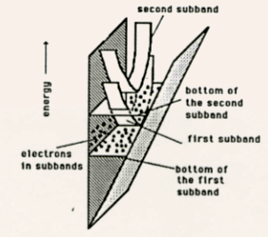
Fig.4.21 Schematic diagram of energy subbands at the semiconductor-insulator
interface (assuming constant effective field approximation).
- For a relatively thick electron gas layer, the number of subbands
is large and the energy difference between the bottoms of the subbands
is small (<< kT).
- For a relatively thin electron gas layer, only the lowest few subbands
are important for electron occupation, and the energy difference between
the bottoms of the subbands may become large compared to the thermal
energy kT.
- In this case, the electron gas is often referred to as a two-dimensional
electron gas (2DEG).
- The density of states D for each subband is given by
 which is a constant and independent of the subband energy Ej => the
overall density of states has a staircase dependence on energy for a
triangular quantum well, which is characteristic for the semiconductor-insulator
interface of an MIS structure.
which is a constant and independent of the subband energy Ej => the
overall density of states has a staircase dependence on energy for a
triangular quantum well, which is characteristic for the semiconductor-insulator
interface of an MIS structure.
- The number of electrons occupying a given subband j can be found by multiplying the density of states D for a single subband by the F-D distribution function, and integrating from Ej to infinity:
| 4 |