-
These states behave acceptor-like or donor-like, depending on the position of the Fermi level at the surface and the amount of band bending, and these are referred to as fast states, since they capture and release the carriers at a fast rate.
-
When the surface potential changes, the charges in the surface states change as well, and leads to a shift in VT and a change in the C-V characteristics.
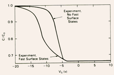
Fig.4.13 The experimental C-V characteristics showing the difference
between them due to the presence of fast surface states.
-
There is a shift of the C-V curve towards the left due to the fast surface states, which changes the flatband voltage.
-
In the equivalent circuit of an MIS structure, the fast surface states can be represented by an additional series combination of an equivalent capacitance Css of the surface states, and an additional resistance Rss, with the time constant RssCss representing the time response of the surface states.
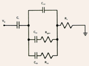
Fig.4.14 The overall high-frequency equivalent circuit for a two-terminal
MIS structure showing the additional components Css-Rss
to account for the effects of fast surface states.
-
Measurements of frequency-dependent MIS capacitance and conductance give information about the density of the surface states.
4.5.2 Ionic Contamination
-
A major difficulty with early MOS devices was the instability of the threshold voltage VT, i.e., it used to vary with bias under elevated temperatures.
-
This happens due to the rearrangement of the mobile ions
 within the oxide, which are introduced into the oxide from
the furnace walls during oxidation.
within the oxide, which are introduced into the oxide from
the furnace walls during oxidation.
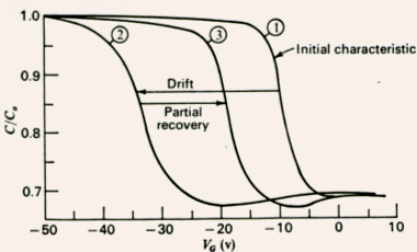
Fig.4.15 Shift in the C-V characteristic after the bias-temperature
stress test due to ionic contamination in the oxide, and its partial
recovery after annealing with gate-substrate shorted.
-
The initial C-V characteristic is marked by (1), while those observed after 30 minutes at 127 C with VG = +10 V applied is marked by (2), and after heating the device for 30 minutes at the
 same
temperature with the gate shorted to the substrate yields characteristic
marked by (3)- this experimental procedure is known as the bias-temperature
stress test.
same
temperature with the gate shorted to the substrate yields characteristic
marked by (3)- this experimental procedure is known as the bias-temperature
stress test.
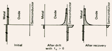
Fig.4.16 Charge distribution during the various stages of the bias-temperature
stress test and post annealing.
-
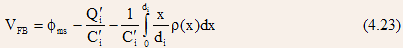
Initially, all the positive ionic charges are located at the metal-SiO2 interface, exerting no influence on Si; after positive gate bias at high temperature, all these ionic charges cluster near the Si-SiO2 interface and induce all the image charges in Si; finally after recovery, the ions create an arbitrary distribution (x) within the oxide, inducing image charges in both the gate and the semiconductor.
-
For any arbitrary distribution of the oxide charges (x), the shift in the flatband voltage

-
can be given by
![]()
where di is the oxide thickness.
-
The menace created by mobile ions is reduced to a large extent in today's technology due to the improvements in the fabrication process.
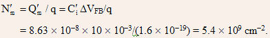
EXAMPLE 4.4: In a two-terminal MIS structure having 40 nm thick oxide, the shift in the flatband voltage after a bias-temperature stress test was found to be 10 mV. Determine the mobile ionic contamination per unit area in the oxide in numbers per unit area.
4.5.3 Radiation-Induced Space Charge
-
A positive space charge is seen to build up in SiO2 films when it is irradiated by ionizing radiation of various kinds, e.g., X-ray, gamma ray, low- and high-energy electron irradiation, etc. (potential danger during ion implantation).
-
The physical origin of this charge is completely different from the ionic contamination.
-
Due to irradiation, EHPs will be generated within the SiO2.
-
In the absence of any electric field within the oxide, these carriers will immediately recombine; however, under a positive applied gate bias, due to the electric field within the SiO2, the generated electrons and holes would separate, with the electron moving towards the metal-SiO2 interface, and the hole moving towards the SiO2-Si interface.
-
Thus, a space charge layer starts to build up within the oxide due to these charges, thus creating an electric field within the oxide, which is opposite to that of the applied field => changes VFB, and, thus, VT.
-
These charges can be eliminated by thermal annealing.
-
A fixed charge is seen to exist within the oxide very near the Si-SiO2 interface, which results in a parallel translation in the C-V characteristics along the voltage axis these charges are called the surface state charges, and the density of these charges per unit area is denoted by

-
These surface states have the following properties:
- It is fixed, i.e., its charge states cannot be changed over a wide variation in the band bending.
- Unchanged under bias-temperature stress test and thermal annealing.
-
It is located within 200
 of the Si-SiO2
interface.
of the Si-SiO2
interface. -
Its density is not significantly altered by the oxide thickness, or by the type or concentration of impurities in Si.
-
Its density is a strong function of the oxidation and annealing conditions, and the orientation of the Si crystal.
-
The ratio o f
 in (111), (110), and (100) Si are in the ratio 3:2:1, and is a
strong function of the oxidation condition.
in (111), (110), and (100) Si are in the ratio 3:2:1, and is a
strong function of the oxidation condition.
-
Popular theory:originates
from the excess ionic Si in the oxide, which
moves into the growing SiO2
layer during the oxidation process.
- can be
reduced by a large extent by H2 heat treatment
4.6 General Expression for the Flatband Voltage VFB
-
The general expression for the flatband voltage VFB can be given by
 where
where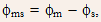 where m is the metal work function and
  is the semiconductor work function;
  is the oxide charges lumped at the Si-SiO2
interface, and
is the oxide charges lumped at the Si-SiO2
interface, and  is any arbitrary distribution of charges within the
oxide.
is any arbitrary distribution of charges within the
oxide.
4.7 Some Advanced Models
4.7.1 Unified Charge Control Model (UCCM) for MIS Capacitors
-
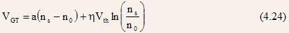
The standard charge control model (SCCM) postulates that the interface inversion charge of electrons qns is proportional to the applied voltage swing VGT = VG -VT.
-
This model is an adequate description of the strong inversion region of the MIS capacitor, but fails for applied voltages near and below VT (i.e., in the depletion and weak inversion regions).
-
A new model has recently been proposed which has been shown to model the device behavior adequately both in the weak and strong inversion regions, and is given as:
 where
where is the permittivity of the gate insulator,
di is the thickness
of the gate insulator,
is the permittivity of the gate insulator,
di is the thickness
of the gate insulator, is an ideality factor, and
  is
a correction to the insulator thickness
related to the shift in the Fermi level
in the inversion layer with respect to the
bottom of the conduction band.
is
a correction to the insulator thickness
related to the shift in the Fermi level
in the inversion layer with respect to the
bottom of the conduction band.
-
Note: Eq.(4.24) does not describe the mobile charge in the accumulation region, however, this region is not important for MOSFET operation.
-
This correction is dependent on the interface electron density, however, it can be approximately taken to be a constant for typical values of the interface electron density.
-
For Si-SiO2 MOS capacitors
 hence, it can usually be assumed that

-
The ideality factor
reflects the gate voltage division between
the insulator layer capacitance Ci
and the depletion layer capacitance Cdep.
-
In the subthreshold regime,

-
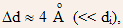
At the onset of strong inversion (VGT = 0), the surface potential Vs has the value

-
Below threshold, we have the following approximate relationship:
-
Note: in general,is
dependent on VGT,
and at low substrate doping levels,
is close to unity near threshold where the
gate depletion width is large (corresponding
to Cdep << Ci).
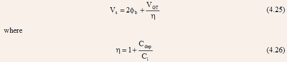
-
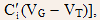
Usually, Cdep can be estimated as follows:
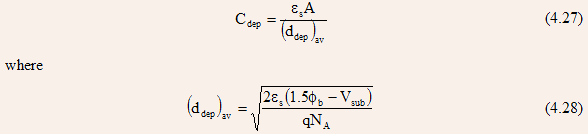 is an average width of the depletion region.
-
Equation (4.24) is an empirical equation, which can be justified by comparing the calculation results with experiments and more precise calculations.
-
Intuitively, the structure of the UCCM expression [Eq.(4.24)] seems reasonable, since in the strong inversion region, it reverts to the simple charge control model [i.e.,

 while in the subthreshold region, it predicts
that the inversion charge is an exponential
function of the applied voltage, as expected.
while in the subthreshold region, it predicts
that the inversion charge is an exponential
function of the applied voltage, as expected.
-
Since UCCM is an empirical model, it is especially important to have a clear and unambiguous procedure for extracting model parameters from experimental data.
-
For the MIS structure, this extraction of parameters is based on the C-V characteristics, which shows a sharp increase in the capacitance (at low frequencies) during the transition from the depletion to the strong inversion region.
-
The voltage at which the derivative of the MIS capacitance reaches its maximum value is very close to the threshold voltage VT.
-
The first derivative of Eq.(4.24) with respect to VGT yields the following unified expression for the metal-channel capacitance per unit area
 valid for all values of applied bias voltage:
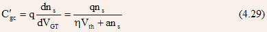
-
The first derivative of this capacitance
| 4 |