4.1 Basic Physics and Band Diagrams for MOS Capacitors
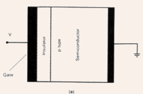
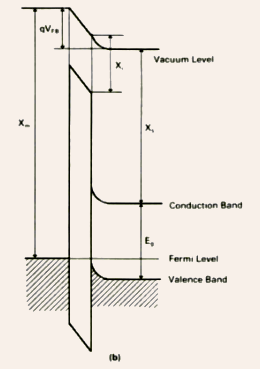
Fig.4.1 (a) The schematic of a two-terminal MIS structure. (b) Band diagram of a two-terminal MIS structure at zero gate voltage, showing accumulation of holes near the surface. VFB is the flatband voltage, Xm is the metal work function, Xi is the electron affinity of the insulator, Xs is the electron affinity of the semiconductor, and Eg is the band gap of the semiconductor.
- Two-terminal metal-insulator-semiconductor (MIS) structure: characteristic crucial to understand the operation of MOSFETs.
-
Assumptions:
-Ideal MIS structure with no charges in the insulator layer and no surface states at the semiconductor-insulator interface.
-The insulator layer has infinite resistivity, thus there is no current across the insulator when a bias voltage is applied => Fermi level constant across the device. -
Some definitions:
-Work function: energy required to remove an electron from the Fermi level to the vacuum level (free space).
-Electron affinity: energy required to remove an electron from the conduction band to the vacuum level.
-
At zero bias voltage, the band bending in the semiconductor layer is determined by the work function difference between the metal and the semiconductor, and it can be compensated by applying a voltage VFB to the gate
![]()
-
Note: this equation for VFB is applicable for an ideal MIS structure; however, if there are charges in the insulator or at the insulator-semiconductor interface, then the gate voltage required to obtain flatband condition would change.
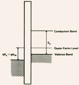
Fig.4.2 The band diagram of the two-terminal MIS structure under the
flatband condition. Vg is the applied gate voltage.
EXAMPLE 4.1: A two-terminal Si MIS structure has a substrate doping of
SOLUTION: Ei EF = kT ln(NA/ni) = 0.026 ln[1016/(1.5 1010)] = 0.35 eV
Therefore, Si work function s = Xs
+ (Eg/2) + (Ei EF)
= 4.05 + 0.56 + 0.35 = 4.96 eV
(a) For Al gate, VFB = 4.1 4.96 = 0.86 V
Note: all these numbers can be equivalently represented either in volts or in electron-volts, depending on whether potential or energy is represented.
(b) ![]() -poly gate, hence, Xm
= Xs = 4.05 eV
-poly gate, hence, Xm
= Xs = 4.05 eV
It is assumed here that the Fermi level of the n+-poly gate is coincident with the conduction band.
Therefore, VFB = 4.05 4.96 = 0.91 V
-
In Fig.4.1(b), note that Ev has come closer to EF near the semiconductor-insulator interface => hole concentration is greater near the interface than that in the bulk => this is referred to as the accumulation regime.
-
In Fig.4.2, note that after the application of a positive VFB to the gate, the bands in the semiconductor become flat => uniform concentration of holes throughout the semiconductor.
-
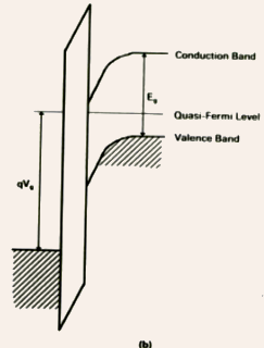
If the gate voltage is further increased, the holes near the insulator-semiconductor interface are pushed back deep into the bulk, leaving behind ionized acceptors near the surface and the bands bend downwards => formation of depletion region near the surface starts => referred to as the depletion regime [Fig.4.3(a)].
-
For even larger positive gate voltage, the band bending near the surface becomes so large that EF becomes closer to EC than to EV => the surface behaves like an n-type material => referred to as the inversion regime [Fig.4.3(b)].
-
Note: the increase in the band bending leads to an exponential increase in the electron concentration near the surface, e.g., an increase in the band bending by the amount of the thermal voltage VTH (= kT/q 26 mV at room temperature), increases the electron concentration by

-
Thus, a large change in the electron concentration near the surface can be accommodated by a small change in the surface potential Vs, and since the induced charge is proportional to the gate voltage Vg, hence, the derivative dVs/dVg becomes small in the inversion regime, whereas this derivative has a large value in the depletion regime.
-
When the difference
 between EF and Ei at the interface becomes equal
and opposite of the bulk potential
between EF and Ei at the interface becomes equal
and opposite of the bulk potential [ =(Ei EF)bulk = VTHln(NA/ni),
where NA is the substrate doping concentration
and ni is the intrinsic carrier concentration],
i.e.,
[ =(Ei EF)bulk = VTHln(NA/ni),
where NA is the substrate doping concentration
and ni is the intrinsic carrier concentration],
i.e.,  it is referred to as the onset of strong inversion.
-
The surface potential Vs is defined as (Ei,bulk Ei,interface)/q.
-
Operating regions:
-
VS < 0 => accumulation
-
 >
Vs > 0 => depletion
>
Vs > 0 => depletion -
 =>
weak inversion
=>
weak inversion -
 =>
strong inversion.
=>
strong inversion.
-
It is assumed that beyond strong inversion, the value of Vs does not change any more and it becomes pegged at
 .
.
-
An alternate definition has been proposed by Tsividis, which states that
 = |dVs/dVg| is quite large
in the weak inversion regime, whereas it becomes relatively small
in the strong inversion region.
= |dVs/dVg| is quite large
in the weak inversion regime, whereas it becomes relatively small
in the strong inversion region.
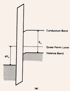
Fig.4.3 The band diagram of a two-terminal MIS structure at (a) depletion
and (b) inversion.
-
Thus, he defines Vs =
 as
the onset of moderate inversion, and strong inversion actually takes
place when Vs is greater than by
several (3-5) VTH.
as
the onset of moderate inversion, and strong inversion actually takes
place when Vs is greater than by
several (3-5) VTH.
-
In today's context, the moderate inversion region (which can extend by 0.5 V or more) is extremely important for low power device applications in analog circuits.
-
However, for the time being, we would stick to the standard definition of strong inversion, and would discuss about moderate inversion later.
-
The surface electron and hole concentrations are given by
![]()
-
Note: at the onset of strong inversion Vs =, and
also, that nsps = => consequence of zero current in the semiconductor
(perpendicular to the semiconductor-insulator interface) => corresponds
to constant (as a function of distance) EF in
the semiconductor.
4.2 Surface Charge
-
The potential distribution in the semiconductor is described by the Poisson equation

 where
the space charge density
where
the space charge density  with n(x) and p(x) expressed respectively as
![]()
-
Note: deep into the bulk, from charge neutrality condition, NA = pp0 np0.
-
Thus,
![]()
-
Using the definition of the electric field F = dV(x)/dx, the above equation can be rewritten as
![]()
-
Integrating this equation with respect to V, one gets

-
Thus,
![]()
-
Introducing the Debye length