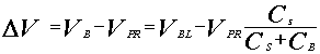
The circuit shown in Figure 30.51 is the simple DRAM circuit. Charge sharing takes place between the two capacitors during read and write operations in the following manner. During the write cycle, is charged or discharged by asserting WL and BL. During the read cycle, charge redistribution takes place between the bit line and the storage capacitance.
(Eq 30.1)
Voltage swing is small; typically around 250mV.
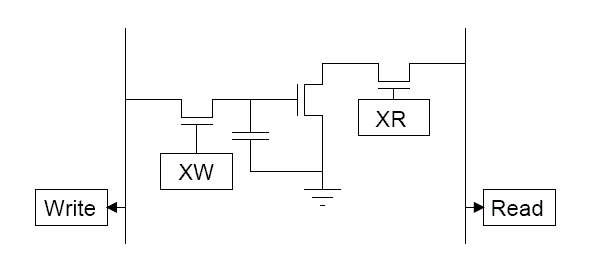
Figure 30.52 shows a simple 3-transistor DRAM cell.
Fig 30.52: 3-Transistor DRAM Cell
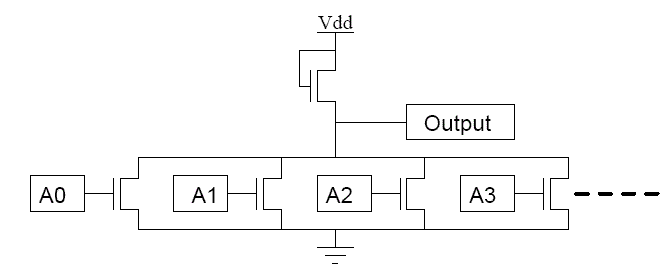
Figure 30.53 shows a very simple address decoder. These address decoders are compulsory in case of main memories. But the cache memories avoid the usage of address decoders. Many other possible architectures are available for address decoding.