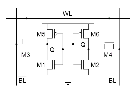
Figure 30.21 shows a standard 6 transistor SRAM cell. The signal designed as is the WORDLINE used to read or write into the cell. and are the data to be written into the cell.
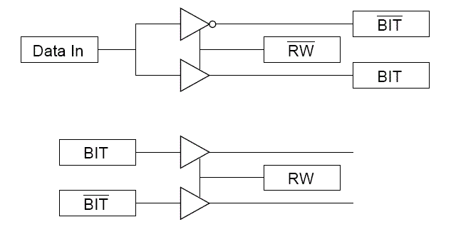
Fig 30.22: Circuit for reading and writing data into cell
The circuits shown in the previous page are used to write and read the data to and from the cell. When a read operation is to be performed,signal is made HIGH and at the same time is made LOW. As a result the data present on the and lines are transferred to the input of the sense amplifier (Sense amplifier operation will be discussed shortly). The sense amplifier then senses the data and gives the output.
During the write operation,is made LOW and is made HIGH. Thus the and will be written onto the and lines respectively.
However the read and write operation on a particular cell takes place only if the cell is enabled by the corresponding row(Word) and column(Digit) lines. It is important to remember that before every read operation, the and are precharged to a voltage (usually VDD/2). During read operation, one of the two BIT ( or ) lines discharges slightly whereas the other line charges to a voltage slightly greater than its precharged value. This difference in these voltages is detected by the sense amplifier to produce and output voltage, which corresponds to te stored value in the cell which is read. Care should be taken in sizing the transistors to ensure that the data stored in the cell does not change its value.