Lecture 19 : Analyzing Delay for various Logic Circuits
19.3 Dynamic Logic Circuits
In case of static CMOS for a fan-in of N, 2N transistors are required. In order to reduce
this, various other design logics were used like pseudo-NMOS logic and pass transistor
logic. However the static power consumption in these cases increased. An alternative to
these design logics is Dynamic logic, which reduces the number of transistors at the
same time keeps a check on the static power consumption.
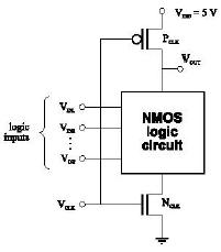
Principle: A block diagram of a dynamic logic circuit is as shown in fig 19.31. This uses NMOS block to
implement its logic
The operation of this circuit can be explained in two modes.
1) Precharge
2) Evaluation
In the precharge mode, the CLK input is at logic 0. This forces the output to logic 1,
charging the load capacitance to VDD. Since the NMOS transistor M1 is off the pull-down
path is disabled. There is no static consumption in this case as there is no direct path
between supply and ground.
In the evaluation mode, the CLK input is at logic 1. Now the output depends on the PDN
block. If there exists a path through PDN to ground (i.e. the PDN network is ON), the
capacitor CL will discharge else it remains at logic 1.As there exists only one path
between the output node and a supply rail, which can only be ground, the load capacitor
can discharge only once and if this happens, it cannot charge until the next precharge
operation. Hence the inputs to the gate can make at most one transition during evaluation
Advantages of dynamic logic circuits:
1) As can be seen, the number of transistors required here are N+2 as compared to 2N in the Static CMOS circuits.
Fig 19.31: Dynamic CMOS Block Diagram
2) This circuit is still a ratioless circuit as in Static case. Hence, progressive sizing
and ordering of the transistors in the PDN block is important.
3) As can be seen, the static power loss is negligible.
Disadvantages of dynamic logic circuits:
1) The penalty paid in such circuits is that the clock must run everywhere to each such block as shown in the diagram.
2) The major problem in such circuits is that the output node is at Vdd till the end of the precharge mode. Now if the CLK in the next block arrives earlier compared to the CLK in this block, or the PDN network in this block takes a longer time to evaluate its output, then the next block will start to evaluate using this erroneous value
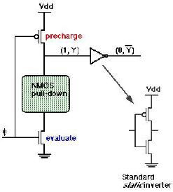
The second part of the disadvantage can be eliminated by using DOMINO CMOS
circuits which are as shown below.
As can be seen the output at the end of precharge is inverted by the inverter to logic 0.
Thus the next block will not be evaluated till this output has been evaluated. As an ending
point, it must be noted that this also has a disadvantage that since at each stage the output
is inverted, the logic must be changed to accommodate this.