Lecture 19 : Analyzing Delay for various Logic Circuits
19.2 Pass Transistor Logic
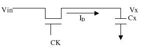
The fundamental building block of
nMOS dynamic logic circuit, consisting of an
nMOS pass transistor is shown in figure 19.21.
The pass transistor MP is driven by the
periodic clock signal and acts as an access
switch to either charge up or down the parasitic
capacitance, Cx, depending on the input signal
Vin. Thus there are 2 possible operations when
the clock signal is active are the logic “1”
transfer( charging up the capacitance Cx to logic
high level) and the logic “0” transfer( charging
down the capacitance Cx to a logic low level). In either case, the output of
Fig 19.21: Pass Transistor Logic Circuit
the depletion load of the nMOS inverter obviously assumes a logic low or high level, depending on the voltage Vx.
The pass transistor MP provides the only current path to the intermediate capacitive node X. when clock signal becomes inactive (clk=0) the pass transistor ceases to conduct and the charge is stored in the parasitic capacitor Cx continues to determine the output level of the inverter.
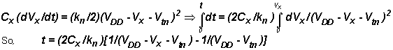
Logic “1” Transfer: Assume that the Vx = 0 initially. A logic "1"level is applied to the input terminal which
corresponds to Vin=VOH=VDD. Now the clock signal at the gate of the pass transistor goes from0 to VDD at t=0. It can be seen that the pass
transistor starts to conduct and operate in
saturation throughout this cycle since VDS=VGS.
Consequently VDS>VGS-Vtn.
Analysis:
The pass transistor operating in
saturation region starts to charge up the
capacitor Cx, thus: