Lecture 19 : Analyzing Delay for various Logic Circuits
19.1 Ratioed Logic
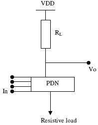
Instead of combination of active pull
down and pull up networks such a gate consists
of an NMOS pull down network that realizes the
logic function and a simple load device. For an
inverter PDN is single NMOS transistor. The
load can be a passive
device, such as a resistor or an active element as a transistor. Let us assume that both PDN and load can be represented as linearized resistors. The operation is as follows: For a low input signal the pull down network is off and the output is high by the load. When the input goes high the driver transistor turns on , and the resulting output voltage is determined by the resistive division between the impedances of pull down and load network:
VOL= RDVDD/(RD+RL)
where RD = pulldown n/w resistance, RL= load resistance.
To keep the low noise margin high it is
important to chose RL>>RD . this style of logic
therefore called ratioed, because a careful
PDN
scaling of impedances(or transistor sizes) is
required to obtain a workable gate. This is in
contrast to the ratioless logic style as
complementary CMOS, where the low and high
level don’t depend upon transistor sizes. As a
satisfactory level we keep RL>=4RD . To
achieve this, (W/L)D/(W/L)L> 4.