Lecture 19 : Analyzing Delay for various Logic Circuits
Contd...
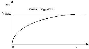
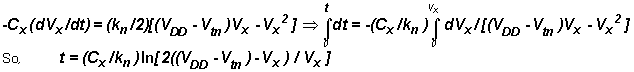
The previous equation for Vx(t) can be solved as-
The variation of the node voltage Vx(t)is plotted as a function of time in fig. 19.22. The
voltage rises from its initial value of 0 and
reaches Vmax =VDD-Vtn after a large time. The
pass transistor will turn off when Vx = Vmax.
Since Vgs= Vtn. Therefore Vx can never attain
VDD during logic 1 transfer. Thus we can use
buffering to overcome this problem.
Logic “0” Transfer: Assume that the Vx=1initially. A logic“0” level is
Fig 19.22: Node Voltage Vx vs t
applied to the input terminal which
corresponds to Vin=1. Now the clock signal
at the gate of the pass transistor goes from 0 to
VDD at t=0. It can be seen that the pass transistor
starts to conduct and operate in linear mode
throughout this cycle and the drain current flows
in the opposite direction to that of charge up.