| 10.3 Self-aligned Silicon Gate Technology |
| When the metal is used as the gate material, then the source and drain are deposited before the gate and thus to align the |
 |
|
gate, mask aligners are used and errors in aligning takes place. In case of polysilicon gate process, the exposed gate oxide(not covered by polysilicon) is etched away and the wafer is subjected to dopant-source or ion-implant which causes source-drain deposition and also these are formed in the regions not covered by polysilicon and thus source and drain donot extend under the gate. This is called self-aligning process. |
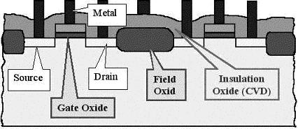
| Figure 10.3: Cross sectional view of MOSFET under Self-algining process |
|
|
| |
| 10.4 Channel Stopper |
| It is used to prevent the channel formation in the subtrate below the field oxide. For example, for a p-substrate, the channel stopper implant would p+ which will increase the magnitude of threshold voltage. |
| Irregular surfaces can cause "step coverage problems" in which a conductor thins and can even break as it crosses a thick to thin oxide boundary. One of the methods used to remove these irregularities is to pre-etch the silicon in areas where the field oxide is to be grown by arround half the final required field oxide thickness. LOCOS (will explain it shortly) oxidation done after this gives the planner field oxide/gate oxide interface. |
| |
| 10.5 Polysilicon Deposition |
| The sheet resistance of undoped polysilicon is 10^8 ohms/cm and it can be reduced to 30 ohm/cm by heavy doping. The advantage of using polysilicon as gate material is its use as further mask to allow precise definition of source and drain. The polysilicon resistance affects the input resistance of the transistor and thus should be small for improving the RC time constant. For this, higher doping concentration is used. |
| |