TEM: Imaging Modes
High-Resolution TEM images
HRTEM analysis helps to understand the growth of the materials, interface morphology and quality of texture, single crystalline nature of the materials, etc. Figure 15.05 displays the typical HRTEM images obtained using TEM.
|
|
|
|
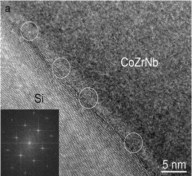
Figure 15.05: HRTEM micrograph of amorphous CoZrNb on Si substrate showing a possible inter-diffusion across the interface of about 2-3 nm [1]. |
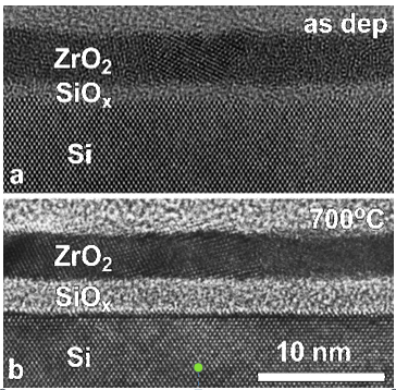
Figure 15.06: The effect of post-deposition annealing under O2 atmosphere on the microstructure of SiOx/ ZrO2 gate dielectric stacks [2]. |
|
|
|
|
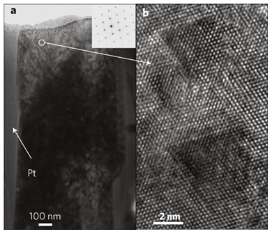
Figure 15.07: Post deformation irradiation defect characterization using high resolution TEM. (a) Low magnification TEM image of a deformed 788 nm diameter copper pillar after FIB lift out and subsequent Ar+ low energy ion milling at 500 eV. (b) Atomic resolution image taken from the area indicated in a, showing ~2-3 nm large SFTs imaged along the (110) projection [3]. |
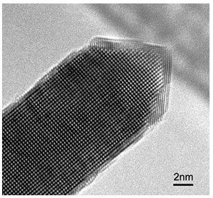
Figure 15.08: High resolution TEM image of RuO2 nanorod [4]. |
Ref.[1]. Li et al, J. Magn. Magn. Mater. 315 (2007) 120.
Ref.[2]. Houssa et al, Semiconductor science and tech. 16 (2000) 306.
Ref.[3]. D. Kiener et al, Nature Materials 10 (2011) 608.
Ref.[4]. http://www-hrem.msm.cam.ac.uk/gallery/