Diffraction mode:
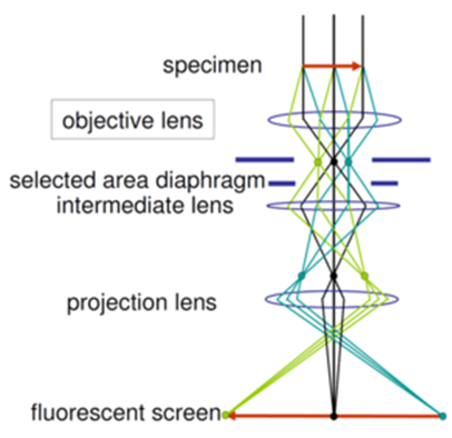
Figure 14.07: Schematic ray diagram of diffraction mode.
This is obtained by intentionally excluding central beam and collecting all diffracted beams as shown in figure below to form the diffraction pattern.
A thin crystalline specimen is subjected to a parallel beam of high-energy electrons. As the wavelength of high-energy electrons is a few thousandths of a nanometer and the spacing between atoms in a solid is about a hundred times larger, the atoms act as a diffraction grating to the electrons, which are diffracted.
As a result, the image on the screen of the TEM will be a series of spots or rings (corresponding to a satisfied diffraction condition of the sample's crystal structure).
SAED is referred to as "selected" because the user can choose part of the specimen to obtain the diffraction pattern.
As a diffraction technique, SAED can be used to identify crystal structures and examine crystal defects. It is similar to X-ray diffraction, but unique in that areas as small as several hundred nanometers in size can be examined. However, X-ray diffraction typically samples areas of several centimeters.
SAED is used primarily in material science and solid state physics. This is one of the most commonly used experimental techniques.