Dark-field imaging mode:

Figure 14.04: (a) TEM bright-field image and related SAED pattern of the CuCr43 composite processed by HPT up to 25 revolutions; (b) dark-field image of the same area obtained by selecting some (111)Cu and (110)Cr lattice reflections (first Debye-Scherrer ring) [3].
Figure 14.04 (a) displays the TEM bright-field image and related SAED pattern of the CuCr43 composite in nanometer range. The dark field image on the Figure 14.04 (b) was obtained by selecting a part of the first ring with a small aperture. This image clearly shows the grain size is in a range of only 10 to 20 nm.
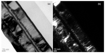
Figure 14.05: (a) TEM bright-field and (b) dark-field couple images of cross-section view of a magnetic tunneling junction shows the contrast from layer by layer [4].
Figure 14.05 displays bright-field and dark-field images of cross-sectional view of magnetic tunnel junction with different contrast from layer by layer.
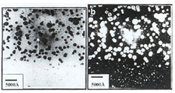
Figure 14.06: (a) Ni-Cu-2-Methoxyethanol colloid electron micrograph at 20 K magnification; 78.4% Ni and 21.6% Cu (a) Bright-field (b) Dark-field [5].
Figure 14.06(a) depicts zone of low contrast forming a cloud around the particles and the cluster (see the arrow) several spherical particles with an average size of 50 nm. This cloud does not allow to see us particles which can be observed in the dark field (Figure 14.05(b)).
Ref.[3]. X. Sauvage et al, Scripta Mater 58 (2008) 1125-1128.
Ref.[4]. http://blog.nus.edu.sg/ngoducthe/science-galery/.
Ref.[5]. GALO CARDENAS-TRIVINO, J. Chil. Chem. Soc. 50 (2005) 603.