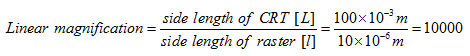
For example, if electron beam is made to scan 10 μm×10 μm raster on the specimen and the corresponding image raster is displayed on CRT screen as 100mm × 100 mm, then linear magnification will be
SEM is able to provide image magnification from about 20× to greater than 100,000×.
Resolutions (Pixels)
Image performance in SEM can be explained on the basis of the picture element or pixel. The amplified signal from the detector makes a minimum spot size of ~ 0.1 mm or 100 micrometer in the CRT. The spot on the CRT mimics the movement of the electron beam on the specimen. Therefore for each of the pixels on the CRT, there is a corresponding pixel on the specimen. The size of specimen pixel (p) is given by ![]() where M = magnification
where M = magnification
Resolution is defined as the smallest separation of two points that microscope can detect as separate entities. In order to resolve two features A and B in Fig 5 they must occupy separate pixels. Therefore working resolution of SEM can be no better than the specimen pixel size ‘p' as given by above equation.
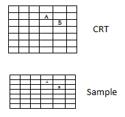
Fig. 5. Raster as array of picture points or pixel on CRT and sample
Resolution of SEM is also controlled by the size of the electron probe scanning the specimen. If the electron probe is larger than the specimen pixel, then the signal from adjacent pixels are merged and the resolution is degraded (Fig 6a).If electron probe is smaller than specimen pixel, then signal will be weaker and noisy (Fig 6b).For optimum performance, probe diameter or sampling volume is made equal to the specimen pixel diameter (Fig 6c).This means that for optimum performance, the probe size should be adjusted as the magnification of the microscope is altered. However, ultimate resolution depends on the smallest probe which can provide adequate signal from the specimen.
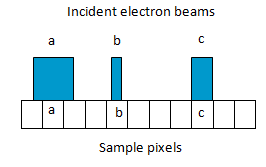
Fig. 6. Size of the electron probe scanning the specimen with respect to specimen pixel.
Sample preparation
Sample preparation for SEM is minimal. This has made SEM more widely used than TEM which requires a very thin specimen and tedious sample preparation procedure. Sample preparation for SEM involves only sizing the specimens to fit SEM specimen holder and removing surface contaminants. This also helps to preserve the surface characteristics for topographic study.
Examples
Fig. 7 shows SEM image of titania samples prepared by precipitation using TiCl2 as precursor. The image shows that the prepared titania sample consisted of particles with wide size distribution and irregular shape. The size of the particles can be measured manually by using the scale given in the figure or by any image analysis software.
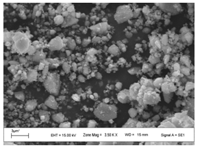
Fig. 7. SEM image of titania samples prepared by precipitation method
Energy dispersive spectrometer (EDS)
In this method, the X-ray generated from interaction of electron beam with sample, is used for chemical analysis of the sample. As high energy electrons strike the sample surface, along with secondary and backscattered electrons, characteristic X-rays are emitted whose wave length depends on nature of atoms in sample. These X-rays can be used to characterize all type of solid materials. The characteristics X-ray is generated when an inner shell electron is knocked out of the atom and the vacant site is filled with electron from outer shell. The excess energy is released and the amount of released energy, corresponding to X-ray range, is characteristics of the particular atom.
For example, if a K shell electron has been knocked out of a molybdenum atom, and vacancy is filled by L electron, then ΔE= 17400 eV, is emitted as Kα X-ray of Mo. The wave length of the corresponding X-ray is ![]() . On the other hand if vacancy is filled by M shell electron, the difference in energy is ΔE ~ 19600 eV. Then the corresponding X-ray emitted is Mo Kβ, λ = 0.063 nm. The K-series lines are more frequently used for analysis. For heavier atoms, the energy required to knockout the K-shell electron increases and consequently exciting the K series line become difficult. In these cases L series and M series of lines can be used which are generated by knocking of L or M shell electrons.
. On the other hand if vacancy is filled by M shell electron, the difference in energy is ΔE ~ 19600 eV. Then the corresponding X-ray emitted is Mo Kβ, λ = 0.063 nm. The K-series lines are more frequently used for analysis. For heavier atoms, the energy required to knockout the K-shell electron increases and consequently exciting the K series line become difficult. In these cases L series and M series of lines can be used which are generated by knocking of L or M shell electrons.
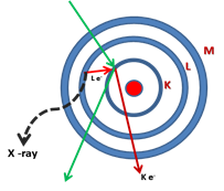
Fig. 8. Emission of X-ray when outer L shell electron fills the K shell electron vacancy
The energy and wavelength of X-rays are different for each atomic species and by measuring them, the elements present in sample can be detected and quantified. From X-ray spectrum following analysis can be done:
-
Measurement of wavelength/energy of each characteristics X-ray emitted. It can be used to determine the elements present in sample. This is a qualitative analysis.
-
Measurement of X-ray of any type emitted per unit time. This corresponds to amount of the element present in sample. This is quantitative analysis.
SEMs are equipped with an energy dispersive spectrometer or EDS detection system which is able to detect and display most of the X-ray spectrum. The detector normally consists of semiconducting silicon or germanium. Since, the X-rays can not be deflected, the detector has to be placed in line of sight of the specimen. In order to collect as many X-rays as possible, the detector is placed near the specimen (20 mm or less from the specimen). It normally occupies a similar position to the secondary electron detector. Each incoming X-rays to the detector excites a number of electrons into the conduction band of the silicon leaving an identical number of positively charged holes in the outer electron shells. The energy required for each of these excitations is only 3.8 eV, consequently the number of electron-hole pairs generated is proportional to the energy of the X-ray photon being detected. For example, an Al Kα X-ray having energy of 1.49 keV, will give rise to approximately [(1.49 x 1000) eV/3.8 eV] = 392 electron hole-pairs. If voltage is applied across the semiconductor, a current will flow as each X-ray is absorbed in the detector and the magnitude of the current will be exactly proportional to the energy of the X-ray. The current which flows between the electrode when an X-ray enters the detector lasts for an extremely short time, less than 1 µs and is normally referred as pulse. Each pulse is amplified and stored in a computer. The EDS spectrum of alumina is shown in Fig 9. It shows the peak due to Al and O.
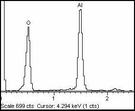
Fig. 9 EDS spectra of alumina
Book reference
• P.J. Goodhew, J. Humphreys, R. Beanland, Electron microscopy and analysis, 3rd ed., Taylor & Francis, 2001
• Y. Leng, Materials Characterization: Introduction to microscopic and spectroscopic methods, John Wiley & Sons, 2008