Scanning electron microscope
SEM is most widely used type of electron microscope for study of microscopic structure. In SEM, image is formed by focused electron beam that scans over the surface area of specimen. The incident beam in SEM is also called electron probe. The incident beam is of typically 10 nm diameter in contrast to beam of TEM which is about 1 μm. In SEM, image is not formed by instantaneous illumination of the whole field as for TEM. SEM is relatively easy to operate and maintain, compared to a TEM. In TEM, unless specimen is made very thin, electrons are strongly scattered within the specimen or even adsorbed rather than transmitted. SEM overcomes this limitation.
Electron–Sample Interactions
The interaction of electron beam with samples results in secondary electrons and backscattered electrons that are detected by standard SEM equipment.
Secondary Electrons: As incoming electrons pass through the specimen, they impart some of their energies to electrons of nearby specimen atom. This causes ionization of the electrons of the specimen atom and slight energy loss and path change of the incident electrons. These ionized electrons then leaves the atom with a very small kinetic energy (5eV) and are termed as secondary electrons. The secondary electrons escape from a volume near the specimen surface, at a depth of 5–50 nm and hence are useful to gain topography related informations.
Backscattered Electrons: Some of the electrons of the incident beam collides with the specimen atoms that falls in the path and are reflected or back scattered. The production of backscattered electrons varies directly with the specimen's atomic number of the specimen. When backscattered electrons are detected, higher atomic number elements appear brighter than lower atomic number elements. This interaction is utilized to differentiate parts of the specimen that have different average atomic number.
Working principle and instrumentation
In SEM, there are several electromagnetic lenses, including condenser lenses and one objective lens. Electromagnetic lenses are for electron probe formation, not for image formation directly, as in TEM. Two condenser lenses reduce the crossover diameter of the electron beam. The objective lens further reduces the cross-section of the electron beam and focuses the electron beam as probe on the specimen surface. Objective lens thus functions like a condenser. This is in contrast to TEM where objective lens does the magnification.
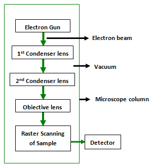
Fig. 3. Schematic diagram illustrating scanning electron microscope
Electron probe or beam is scanned across the specimen and the procedure is known as Raster scanning. Raster scanning causes the beam to sequentially cover a rectangular area on the specimen. The signal electrons emitted from the specimen are collected by the detector, amplified and used to reconstruct the image according to one-to-one correlation between scanning points on the specimen and picture points on the screen of cathode ray tube (CRT). CRT converts the electronic signals to a visual display.
Everhart–Thornley is commonly used detector in SEM. It consist of scintillated photo multiplier system. As electrons strike the scintillator, that is a phosphor, photons are emitted. The photon is transmitted through light pipe into a PMT which converts the photon into pulses of electrons, which is amplified and used to modulate the intensity of CRT.
Magnification and Resolutions
Magnification
In SEM, image is not magnified by any lens as opposed to TEM where magnification is determined by power of the objective lens. Magnification of SEM is determined by the ratio of the linear size of the display screen to the linear size of the specimen area being scanned. Raster displayed on the CRT is larger than the corresponding Raster scanned by the electron beam on the specimen (Fig 4). The linear magnification is given by
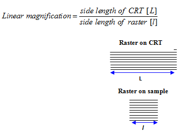
Fig. 4 . Raster on sample and corresponding raster on CRT