- In addition to the knowledge of carrier concentrations, the collisions
of the charge carriers with the lattice and with the impurity atoms
(or ions) under electric and/or magnetic fields must be accounted for,
in order to compute the current flow through the device.
- These processes will affect the ease (mobility) with which
carriers move within a lattice.
- These collision and scattering processes depend on temperature, which affects the thermal motion of the lattice atoms and the velocity of the carriers.
- Even at thermal equilibrium, the carriers are in a constant motion
within the lattice.
- At room temperature, the thermal motion of an individual electron
may be visualized as random scattering from lattice atoms, impurities,
other electrons, and defects.
- There is no net motion of the group of n
 electrons/cm3
over any period of time, since the scattering is random, and there is
no preferred direction of motion for the group of electrons and no net
current flow.
electrons/cm3
over any period of time, since the scattering is random, and there is
no preferred direction of motion for the group of electrons and no net
current flow.
- However, for an individual electron, this is not true the probability
of an electron returning to its starting point after time t is negligibly
small.
- Now, if an electric field
 is applied in the x-direction, each electron experiences a net force
q
from the field.
is applied in the x-direction, each electron experiences a net force
q
from the field.
- This will create a net motion of group in the x-direction, even though
the force may be insufficient to appreciably alter the random path of
an individual electron.
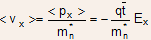
- If
 is the x-component of the total momentum of the group, then the force
of the field on the n
is
is the x-component of the total momentum of the group, then the force
of the field on the n
is
 (2.18)
Note: this expression indicates a constant acceleration in the x-direction, which realistically cannot happen.
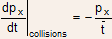
- In steady state, this acceleration is just balanced by the deceleration
due to the collisions.
- Thus, while the steady field
does produce a net momentum
 ,
for steady state current flow, the net rate of change of momentum must
be zero when collisions are included.
,
for steady state current flow, the net rate of change of momentum must
be zero when collisions are included.
- Note: the collision processes are totally random, thus, there is a
constant probability of collision at any time for each electron.
- Consider a group of
 electrons at time t = 0, and define N(t) as the number of electrons
that have not undergone a collision by time t
electrons at time t = 0, and define N(t) as the number of electrons
that have not undergone a collision by time t
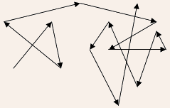
Fig.2.7 The random thermal motion of an individual electron, undergoing random scattering. - The rate of decrease of N(t) at any time t is proportional to the
number left unscattered at t, i.e.
 (2.19)
where is the constant of proportionality.
- The solution is an exponential function
 (2.20)
and represents the mean time between scattering events, called the mean
free time.
represents the mean time between scattering events, called the mean
free time.
- The probability that any electron has a collision in time interval
dt is dt/
, thus, the differential change in
due to collisions in time dt is
 (2.21)
- Thus, the rate of change of
due to the decelerating effect of collisions is
 (2.22)
- For steady state, the sum of acceleration and deceleration effects
must be zero, thus,
 (2.23)
- The average momentum per electron (averaged over the entire group
of electrons) is
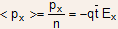 (2.24)
- Thus, as expected for steady state, the electrons would have on the
average a constant net velocity in the -x-direction
 (2.25)
- This speed is referred to as the drift speed, and, in general, it
is usually much smaller than the random speed due to thermal motion
 .
.
- The current density resulting from this drift
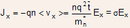 (2.26)
- This is the familiar Ohm's law with
 being
the conductivity of the sample, which can also be written as
being
the conductivity of the sample, which can also be written as  ,
with
,
with is
defined as the electron mobility
is
defined as the electron mobility
(in ),
and it describes the ease with which electrons drift in the material.
),
and it describes the ease with which electrons drift in the material.
- The mobility can also be expressed as the average drift velocity per
unit electric field, thus
 with the negative sign denoting a positive value for mobility since
electrons drift opposite to the direction of the electric field.
with the negative sign denoting a positive value for mobility since
electrons drift opposite to the direction of the electric field.
- The total current density can be given by
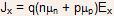 (2.27) when both electrons and holes contribute to the current conduction;
on the other hand, for predominantly n-type or p-type samples, respectively
the first or the second term of the above equation dominates.
(2.27) when both electrons and holes contribute to the current conduction;
on the other hand, for predominantly n-type or p-type samples, respectively
the first or the second term of the above equation dominates.
Note: both electron and hole drift currents are in the same direction, since holes (with positive charges) move along the direction of the electric field, and electrons (with negative charges) drift opposite to the direction of the electric field.
- Since GaAs has a strong curvature of the E-k diagram at the bottom
of the conduction band, the electron effective mass in GaAs is very
small
 the
electron mobility in GaAs is very high since
the
electron mobility in GaAs is very high since  is inversely proportional to
  .
.
- The other parameter in the mobility expression, i.e., (the
mean free time between collisions) is a function of temperature and
the impurity concentration in the semiconductor.
- For a uniformly doped semiconductor bar of length L, width w, and
thickness t, the resistance R of the bar can be given by
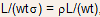 where
where  is
the resistivity.
is
the resistivity.
- The two main scattering events that influence electron and hole motion
(and, thus, mobility) are the lattice scattering and the impurity
scattering.
- All lattice atoms vibrate due to temperature and can scatter carriers
due to collisions.
- These collective vibrations are called phonons, thus lattice scattering
is also known as phonon scattering.
- With increasing temperature, lattice vibrations increase, and the
mean free time between collisions decreases mobility
decreases (typical dependence
 ).
).
- Scattering from crystal defects and ionized impurities dominate at
low temperatures.
- Since carriers moving with low velocity (at low temperature) can get
scattered more easily by ionized impurities, this kind of scattering
causes a decrease in carrier mobility with decreasing temperature (typical
dependence
 ).
).
- Note: the scattering probability is inversely proportional to the
mean free time (and to mobility), hence, the mobilities due to two or
more scattering events add inversely:
 (2.28)
- Thus, the mechanism causing the lowest mobility value dominates.
- Mobility also decreases with increasing doping, since the ionized
impurities scatter carriers more (e.g.,
for intrinsic Si is 1350
 at 300 K, whereas with a donor doping of
  ,
n drops to 700 ).
,
n drops to 700 ).
- For small electric fields, the drift current increases linearly with
the electric field, since
 is
a constant.
is
a constant.
- However, for large electric fields (typically >
 ),
the current starts to show a sublinear dependence on the electric field
and eventually saturates for very high fields.
),
the current starts to show a sublinear dependence on the electric field
and eventually saturates for very high fields.
- Thus, becomes a function of the electric field, and this is known
as the hot carrier effect, when the carrier drift velocity becomes comparable
to its thermal velocity.
- The maximum carrier drift velocity is limited to its mean thermal
velocity (typically
 ),
beyond which the added energy imparted by the electric field is absorbed
by the lattice (thus generating heat) instead of a corresponding increase
in the drift velocity.
),
beyond which the added energy imparted by the electric field is absorbed
by the lattice (thus generating heat) instead of a corresponding increase
in the drift velocity.
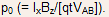
- An extremely important measurement procedure for determining the majority
carrier concentration and mobility.
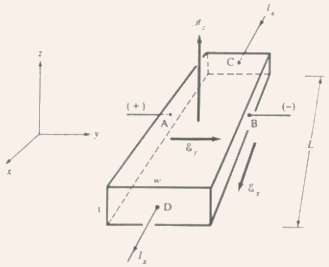
Fig.2.8 The experimental setup for the Hall Effect measurement.
- If a magnetic field is applied perpendicular to the direction of carrier
flow, the path of the carriers get deflected due to the Lorentz force
experienced by the carriers, which can be given by
F = q(E + v x B) (2.29)
- Thus, the holes will get deflected towards the -y-direction, and
establish an electric field along the y-direction, such that in steady
state

- The establishment of this electric field is known as the Hall effect,
and the resulting voltage
 is called the Hall voltage.
- Using the expression for the drift current,
 is called the Hall coefficient.
- A measurement of the Hall voltage along with the information for magnetic
field and current density gives the majority carrier concentration
- Also, the majority carrier mobility
 can be obtained from a measurement of the resistivity
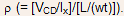
- This experiment can be performed to obtain the variation of majority
carrier concentration and mobility as a function of temperature.
- For n-type samples, the Hall voltage and the Hall coefficient are
negative a
common diagnostic tool for obtaining the sample type.
- Note: caution should be exercised for near intrinsic samples.
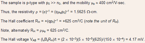
EXAMPLE 2.4: A sample of Si is doped with
SOLUTION:
- In equilibrium, there is no external excitation except a constant
temperature, no net transfer of energy, no net carrier motion, and no
net current transport.
- An important condition for equilibrium is that no discontinuity or
gradient can arise in the equilibrium Fermi level EF.
- Assume two materials 1 and 2 (e.g., n- and p-type regions, dissimilar
semiconductors, metal and semiconductor, two adjacent regions in a nonuniformly
doped semiconductor) in intimate contact such that electron can move
between them.
- Assume materials 1 and 2 have densities of state N1(E) and N2(E),
and F-D distribution functions f1(E) and f2(E) respectively at any energy
E.
- The rate of electron motion from 1 to 2 can be given byrate from 1 to 2 N1(E)f1(E) . N2(E)[1 f2(E)] (2.30)and the rate of electron motion from 2 to 1 can be given byrate from 2 to 1 N2(E)f2(E) . N1(E)[1 f1(E)] (2.31)" At equilibrium, these two rates must be equal, which gives f1(E) = f2(E) => EF1 = EF2 => dEF/dx = 0; thus, the Fermi level is constant at equilibrium, or, in other words, there cannot be any discontinuity or gradient in the Fermi level at equilibrium.
-
2.1 Electrons move in a crystal as wave packets with a group velocity
2.2 Some semiconductors of interest have the dependence of its
energy E with respect to the wave vector k, given by ![]() is
the effective mass for E = 0, k is the wave vector, and
is
the effective mass for E = 0, k is the wave vector, and ![]() is
a constant. Calculate the dependence of the effective mass
is
a constant. Calculate the dependence of the effective mass ![]() on
energy.
on
energy.
2.3 Determine the equilibrium recombination constant r for Si
and GaAs, having equilibrium thermal generation rates of ![]() respectively, and intrinsic carrier concentrations of
respectively, and intrinsic carrier concentrations of ![]() respectively.
Comment on the answers. Will
respectively.
Comment on the answers. Will ![]() change
with doping at equilibrium?
change
with doping at equilibrium?
2.4 The relative dielectric constant for GaP is 10.2 and the
electron effective mass is ![]() Calculate
the approximate ionization energy of a donor atom in GaP.
Calculate
the approximate ionization energy of a donor atom in GaP.
2.5 Show that the probability that a state ![]() above
the Fermi level
above
the Fermi level ![]() is
occupied is the same as the probability that a state
is
occupied is the same as the probability that a state ![]() below
below
![]() is
empty.
is
empty.
2.6 Derive an expression relating the intrinsic level ![]() to
the center of the band gap
to
the center of the band gap ![]() and
compute the magnitude of this displacement for Si and GaAs at 300 K.
Assume
and
compute the magnitude of this displacement for Si and GaAs at 300 K.
Assume ![]() respectively.
respectively.
2.7 Show that in order to obtain maximum resistivity in a GaAs
sample ![]() it
has to be doped slightly p-type. Determine this doping concentration.
Also, determine the ratio of the maximum resistivity to the intrinsic
resistivity.
it
has to be doped slightly p-type. Determine this doping concentration.
Also, determine the ratio of the maximum resistivity to the intrinsic
resistivity.
2.8 A GaAs sample (use the date given in Problem 2.7) is doped
uniformly with ![]() out
of which 70% occupy Ga sites, and the rest 30% occupy As sites. Assume
100% ionization and T = 300 K.
out
of which 70% occupy Ga sites, and the rest 30% occupy As sites. Assume
100% ionization and T = 300 K.
a) Calculate the equilibrium electron and hole concentrations ![]()
b) Clearly draw the equilibrium band diagram, showing the position of
the Fermi level ![]() with
respect to the intrinsic level
with
respect to the intrinsic level ![]() ,
assuming that
,
assuming that ![]() lies
exactly at midgap.
lies
exactly at midgap.
c) Calculate the percentage change in conductivity after doping as compared
to the intrinsic case.
2.9 A Si sample is doped with ![]() donor
atoms. Determine the minimum temperature at which the sample becomes
intrinsic. Assume that at this minimum temperature, the free electron
concentration does not exceed by more than 1% of the donor concentration
(beyond its extrinsic value). For
donor
atoms. Determine the minimum temperature at which the sample becomes
intrinsic. Assume that at this minimum temperature, the free electron
concentration does not exceed by more than 1% of the donor concentration
(beyond its extrinsic value). For ![]()
2.10 Since the event of collision of an electron in a lattice
is a truly random process, thus having a constant probability of collision
at any given time, the number of particles left unscattered at time
t, ![]() Hence,
show that if there are a total of i number of scattering events, each
with a mean free time of
Hence,
show that if there are a total of i number of scattering events, each
with a mean free time of ![]() then
the net electron mobility
then
the net electron mobility ![]() can
be given by
can
be given by ![]() where
where ![]() is
the mobility due to the ith scattering event.
is
the mobility due to the ith scattering event.
2.11 A Ge sample is oriented in a ![]() magnetic
field (refer to Fig.2.8). The current is 4 mA, and the sample dimensions
are w = 0.25 mm,
magnetic
field (refer to Fig.2.8). The current is 4 mA, and the sample dimensions
are w = 0.25 mm,
t = 50 ![]() m,
and L = 2.5 mm. The following data are taken:
m,
and L = 2.5 mm. The following data are taken: ![]() Find
the type and concentration of the majority carrier, and its mobility.
Hence, compute the net relaxation time for the various scattering events,
assuming
Find
the type and concentration of the majority carrier, and its mobility.
Hence, compute the net relaxation time for the various scattering events,
assuming ![]()
2.12 In the Hall effect experiment, there is a chance that the
Hall Probes A and B (refer to Fig.2.8) are not perfectly aligned, which
may give erroneous Hall voltage readings. Show that the true Hall voltage![]() can be obtained from two measurements of
can be obtained from two measurements of ![]() with
the magnetic field first in the +z-direction, and then in the z-direction.
with
the magnetic field first in the +z-direction, and then in the z-direction.