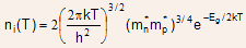
- The F-D distribution function can be used to calculate the electron
and hole concentrations in semiconductors, if the densities of available
states in the conduction and valence bands are known.
- In equilibrium, the concentration of electrons in the conduction band
can be given by
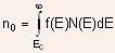 (2.8)
(2.8)
where N(E)dE is the density of available states/cm3 in the energy range dE.
- Note: the upper limit of is theoretically not proper, since the conduction band does not extend to infinite energies; however, since f(E) decreases rapidly with increasing E, the contribution to this integral for higher energies is negligible.
- Using the solution of
 's
wave equation under periodic boundary conditions, it can be shown that
's
wave equation under periodic boundary conditions, it can be shown that
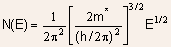 (2.9)
(2.9)
- Thus, N(E) increases with E, however, f(E) decreases rapidly with
E, thus, the product f(E)N(E) decreases rapidly with E, and very few
electrons occupy states far above the conduction band edge, i.e., most
electrons occupy a narrow energy band near the conduction band edge.
- Similarly, the probability of finding an empty state in the valence
band [1 - f(E)] decreases rapidly below
 ,
and most holes occupy states near the top of the valence band.
,
and most holes occupy states near the top of the valence band.
- Thus, a mathematical simplification can be made assuming that all
available states in the conduction band can be represented by an effective
density of states NC located at the conduction band edge
 and using Boltzmann approximation.
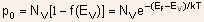
Thus,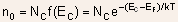 (2.10)
where .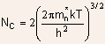
- Note: as (
-
 )
decreases, i.e., the Fermi level moves closer to the conduction band,
the electron concentration increases.
)
decreases, i.e., the Fermi level moves closer to the conduction band,
the electron concentration increases. - By similar arguments,
 (2.11)
where is the effective density of states located at the valence band edge
.
is the effective density of states located at the valence band edge
.
- Note: the only terms separating the expressions for
 and
are the effective masses of electrons (
and
are the effective masses of electrons ( ) and holes (
 ) respectively, and since , hence, .
- Thus, as (
- )
decreases, i.e., the Fermi level moves closer to the valence band edge,
and the hole concentration increases.
- These equations for
 and
and  are valid in equilibrium, irrespective of the material being intrinsic
or doped.
are valid in equilibrium, irrespective of the material being intrinsic
or doped.
- For intrinsic material
lies at an intrinsic level
 (very near the middle of the band gap), and the intrinsic electron and
hole concentrations are given by
(very near the middle of the band gap), and the intrinsic electron and
hole concentrations are given by
 and (2.12)
 - Note: At equilibrium, the product
is a constant for a particular material and temperature, even though
the doping is varied,
i.e.,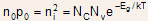 (2.13)
- This equation gives an expression for the intrinsic carrier concentration
ni as a function of ,
,
and temperature:
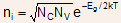 (2.14)
- These relations are extremely important, and are frequently used for
calculations.
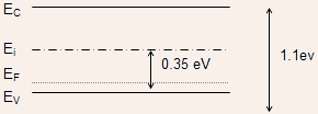
- Note: if
were to be equal to ,
then would
have been exactly at mid gap (i.e., -
= -
=
 /2).
/2).
- However, since
,
is displaced slightly from mid gap (more for GaAs than that for Si).
- Alternate expressions for
and :
 and (2.15)
- Note: the electron concentration is equal to ni when
is at ,
and n0 increases exponentially as
moves away from
towards the conduction band.
- Similarly, the hole concentration
varies from
 to larger values as
moves from
towards the valence band.
to larger values as
moves from
towards the valence band.
EXAMPLE 2.3: A Si sample is doped with
SOLUTION: Since B (trivalent) is a p-type dopant in Si, hence, the material will be predominantly p-type, and since
- The intrinsic carrier concentration has a strong temperature dependence,
given by
 (2.16)
- Thus, explicitly, ni is proportional to T3/2 and to e 1/T, however,
Eg also has a temperature dependence (decreasing with increasing temperature,
since the interatomic spacing changes with temperature).
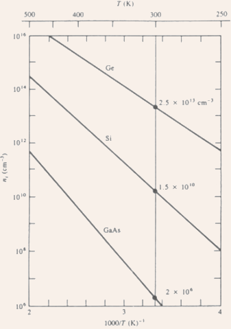
Fig.2.5 The intrinsic carrier concentration as a function of inverse temperature for Si, Ge, and GaAs.
- As
changes with temperature, so do
and .
- With
and T given, the unknowns are the carrier concentrations and the Fermi
level position with respect to
one of these quantities must be given in order to calculate the other.
- Example: Si doped with
 donors (
 ).
).
- At very low temperature, negligible intrinsic EHPs exist, and all
the donor electrons are bound to the donor atoms.
- As temperature is raised, these electrons are gradually donated to
the conduction band, and at about 100 K (1000/T = 10), almost all these
electrons are donated
 this
temperature range is called the ionization region.
this
temperature range is called the ionization region.
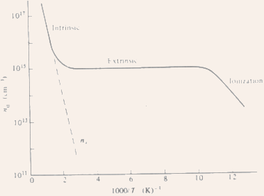
Fig.2.6 Variation of carrier concentration with inverse temperature clearly showing the three regions: ionization, extrinsic, and intrinsic.
- Thus,
remains virtually constant with temperature for a wide range of temperature
(called the extrinsic region), until the intrinsic carrier concentration
ni starts to become comparable to .
- For high temperatures, >>
,
and the material loses its extrinsic property (called the intrinsic
region).
- Note: in the intrinsic region, the device loses its usefulness => determines the maximum operable temperature range.
- Semiconductors can be doped with both donors ()
and acceptors (
 )
simultaneously.
)
simultaneously.
- Assume a material doped with >
predominantly
n-type
lies above acceptor
level Ea completely full, however, with
above ,
the hole concentration cannot be equal to .
- Mechanism:
- Electrons are donated to the conduction band from the donor level

- An acceptor state gets filled by a valence band electron, thus
creating a hole in the valence band.
- An electron from the conduction band recombines with this hole.
- Extending this logic, it is expected that the resultant concentration
of electrons in the conduction band would be
instead of .
- This process is called compensation.
- Electrons are donated to the conduction band from the donor level
- By compensation, an n-type material can be made intrinsic (by making
= )
or even p-type (for >).
Note: a semiconductor is neutral to start with, and, even after doping, it remains neutral (since for all donated electrons, there are positively charged ions ( );
and for all accepted electrons (or holes in the valence band), there
are negatively charged ions (
);
and for all accepted electrons (or holes in the valence band), there
are negatively charged ions ( ).
). - Therefore, the sum of positive charges must equal the sum of negative
charges, and this governing relation,
given by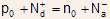 (2.17) is referred to as the equation for space charge neutrality.
- This equation, solved simultaneously with the law of mass action (given
by
 ) gives the information about the carrier concentrations.
Note: for , .
.