- Thus, the electrons in the conduction band are free to move about
via the many available empty states.
- Corresponding problem of charge transport in the valence band is slightly
more complex.
- Current transport in the valence band can be accounted for by keeping
track of the holes themselves.
- In a filled band, all available energy states are occupied.
- For every electron moving with a given velocity, there is an equal
and opposite electron motion somewhere else in the band.
- Under an applied electric field, the net current is zero, since for
every electron j moving with a velocity
 ,
there is a corresponding electron
,
there is a corresponding electron  moving
with a velocity -.
moving
with a velocity -.
- In a unit volume, the current density J can be given by
 (filled band) (2.2)
where N is the number of in the band, and q is the electronic charge.
- Now, if the
 electron is removed and a hole is created in the valence band, then
the net current density
electron is removed and a hole is created in the valence band, then
the net current density
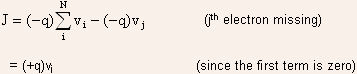
- Thus, the current contribution of the empty state (hole), obtained
by removing the jth electron, is equivalent to that of a positively
charged particle with velocity .
- Note that actually this transport is accounted for by the motion of
the uncompensated electron
having a charge of q and moving with a velocity .
- Its current contribution (- q)(- )
is equivalent to that of a positively charged particle with velocity
+.
- For simplicity, therefore, the empty states in the valence band are
called holes, and they are assigned positive charge and positive mass.
- The electron energy increases as one moves up the conduction band,
and electrons gravitate downward towards the bottom of the conduction
band.
- On the other hand, hole energy increases as one moves down the valence
band (since holes have positive charges), and holes gravitate upwards
towards the top of the valence band.
- The "wave-particle" motion of electrons in a lattice is
not the same as that for a free electron, because of the interaction
with the periodic potential of the lattice.
- To still be able to treat these particles as "free", the
rest mass has to be altered to take into account the influence of the
lattice.
- The calculation of effective mass takes into account the shape of
the energy bands in three-dimensional k-space, taking appropriate averages
over the various energy bands.
- The effective mass of an electron in a band with a given (E,k) relation
is given by
 (2.4)
(2.4)
EXAMPLE 2.1: Find the dispersion relation for a free electron, and, thus, observe the relation between its rest mass and effective mass.
SOLUTION: For a free electron, the electron momentum is
Note: for severely non-parabolic band structures, the effective mass may become a function of energy, however, near the minima of the conduction band and towards the maxima of the valence band, the band structure can be taken to be parabolic, and, thus, an effective mass, which is independent of energy, may be obtained.
- Thus, the effective mass is an inverse function of the curvature
of the E-k diagram: weak curvature gives large mass, and strong curvature
gives small mass.
- Note that in general, the effective mass is a tensor quantity, however,
for parabolic bands, it is a constant.
- Another interesting feature is that the curvature
 is positive at the conduction band minima, however, it is negative
at the valence band maxima.
is positive at the conduction band minima, however, it is negative
at the valence band maxima.
- Thus, the electrons near the top of the valence band have negative
effective mass.
- Valence band electrons with negative charge and negative mass move
in an electric field in the same direction as holes with positive
charge and positive mass.
- Thus, the charge transport in the valence band can be fully accounted
for by considering hole motion alone.
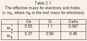
- The electron and hole effective masses are denoted by
 and
and respectively.
- A perfect semiconductor crystal with no impurities or lattice defects.
- No carriers at 0 K, since the valence band is completely full and
the conduction band is completely empty.
- For T > 0 K, electrons are thermally excited from the valence
band to the conduction band (EHP generation).
- EHP generation takes place due to breaking of covalent bonds
 required
energy =
required
energy = .
.
- The excited electron becomes free and leaves behind an empty state
(hole).
- Since these carriers are created in pairs, the electron concentration
(
 )
is always equal to the hole concentration (
)
is always equal to the hole concentration ( ),
and each of these is commonly referred to as the intrinsic carrier
concentration (
),
and each of these is commonly referred to as the intrinsic carrier
concentration ( ).
).
- Thus, for intrinsic material n = p =.
- These carriers are not localized in the lattice; instead they spread
out over several lattice spacings, and are given by quantum mechanical
probability distributions.
- Note: ni = f(T).
- To maintain a steady-state carrier concentration, the carriers must
also recombine at the same rate at which they are generated.
- Recombination occurs when an electron from the conduction band makes
a transition (direct or indirect) to an empty state in the valence
band, thus annihilating the pair.
- At equilibrium,
 =
= ,
where
and
are the generation and recombination rates respectively, and both
of these are temperature dependent.
,
where
and
are the generation and recombination rates respectively, and both
of these are temperature dependent.
- (T)
increases with temperature, and a new carrier concentration ni is
established, such that the higher recombination rate (T)
just balances generation.
- At any temperature, the rate of recombination is proportional to
the equilibrium concentration of electrons and holes, and can be given
by
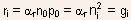 (2.5)
(2.5)
where is a constant of proportionality (depends on the mechanism by which
recombination takes place).
is a constant of proportionality (depends on the mechanism by which
recombination takes place).
- In addition to thermally generated carriers, it is possible to create
carriers in the semiconductor by purposely introducing impurities
into the crystal doping.
- Most common technique for varying the conductivity of semiconductors.
- By doping, the crystal can be made to have predominantly electrons
(n-type) or holes (p-type).
- When a crystal is doped such that the equilibrium concentrations
of electrons (n0) and holes (p0) are different from the intrinsic
carrier concentration (ni), the material is said to be extrinsic.
- Doping creates additional levels within the band gap.
- In Si, column V elements of the periodic table (e.g., P, As, Sb)
introduce energy levels very near (typically 0.03-0.06 eV) the conduction
band.
- At 0 K, these levels are filled with electrons, and very little
thermal energy (50 K to 100 K) is required for these electrons to
get excited to the conduction band.
- Since these levels donate electrons to the conduction band, they
are referred to as the donor levels.
- Thus, Si doped with donor impurities can have a significant number
of electrons in the conduction band even when the temperature is not
sufficiently high enough for the intrinsic carriers to dominate, i.e.,
 >>
,
>>
,
 n-type
material, with electrons as majority carriers and holes as
minority carriers.
n-type
material, with electrons as majority carriers and holes as
minority carriers.
- In Si, column III elements of the periodic table (e.g., B, Al, Ga,
In) introduce energy levels very near (typically 0.03-0.06 eV) the
valence band.
- At 0 K, these levels are empty, and very little thermal energy (50
K to 100 K) is required for electrons in the valence band to get excited
to these levels, and leave behind holes in the valence band.
- Since these levels accept electrons from the valence band, they
are referred to as the acceptor levels.
- Thus, Si doped with acceptor impurities can have a significant number
of holes in the valence band even at a very low temperature, i.e.,
>>
, p-type
material, with holes as majority carriers and electrons as minority
carriers.
- The extra electron for column V elements is loosely bound and it
can be liberated very easilyionization;
thus, it is free to participate in current conduction.
- Similarly, column III elements create holes in the valence band,
and they can also participate in current conduction.
- Rough calculation of the ionization energy can be made based on
the Bohr's model for
 atoms, considering the loosely bound electron orbiting around the
tightly bound core electrons. Thus,
atoms, considering the loosely bound electron orbiting around the
tightly bound core electrons. Thus,
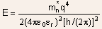 (2.6)where
 is
the relative permittivity of Si.
is
the relative permittivity of Si.
EXAMPLE 2.2: Calculate the approximate donor binding energy for Si ( r = 11.7,
SOLUTION: From Eq.(2.6), we have
Note: The effective mass used here is an average of the effective mass in different crystallographic directions, and is called the "conductivity effective mass" with values of 1.28
- In III-V compounds, column VI impurities (e.g., S, Se, Te) occupying
column V sites act as donors. Similarly, column II impurities (e.g.,
Be, Zn, Cd) occupying column III sites act as acceptors.
- When a column IV material (e.g., Si, Ge) is used to dope III-V compounds,
then they may substitute column III elements (and act as donors), or
substitute column V elements (and act as acceptors)amphoteric
dopants.
- Doping creates a large change in the electrical conductivity, e.g.,
with a doping of
 ,
the resistivity of Si changes from 2 x
,
the resistivity of Si changes from 2 x 
 -cm
to 5 -cm.
-cm
to 5 -cm.
- For the calculation of semiconductor electrical properties and analyzing
device behavior, it is necessary to know the number of charge carriers/cm3
in the material.
- The majority carrier concentration in a heavily doped material is
obvious, since for each impurity atom, one majority carrier is obtained.
- However, the minority carrier concentration and the dependence of
carrier concentrations on temperature are not obvious.
- To obtain the carrier concentrations, their distribution over the
available energy states is required.
- These distributions are calculated using statistical methods.
- Electrons in solids obey Fermi-Dirac (FD) statistics.
- This statistics accounts for the indistinguishability of the electrons,
their wave nature, and the Pauli exclusion principle.
- The Fermi-Dirac distribution function f(E) of electrons over a range of allowed energy levels at thermal equilibrium can be given by
- This gives the probability that an available energy state at E will be occupied by an electron at an absolute temperature T.
 is called the Fermi level and is a measure of the average energy of
the electrons in the latticean
extremely important quantity for analysis of device behavior.
is called the Fermi level and is a measure of the average energy of
the electrons in the latticean
extremely important quantity for analysis of device behavior.
- Note: for (E -)
> 3kT (known as Boltzmann approximation), f(E)
 exp[
- (E- )/kT]
this
is referred to as the Maxwell-Boltzmann (MB) distribution (followed
by gas atoms).
exp[
- (E- )/kT]
this
is referred to as the Maxwell-Boltzmann (MB) distribution (followed
by gas atoms).
- The probability that an energy state at
will be occupied by an electron is 1/2 at all temperatures.
- At 0 K, the distribution takes a simple rectangular form, with all
states below
occupied, and all states above
empty.
- At T > 0 K, there is a finite probability of states above
to be occupied and states below
to be empty.
- The F-D distribution function is highly symmetric, i.e., the probability
f(
+
 )
that a state E above
is filled is the same as the probability [1- f(
-
)] that a state E below
is empty.
)
that a state E above
is filled is the same as the probability [1- f(
-
)] that a state E below
is empty.
- This symmetry about EF makes the Fermi level a natural reference
point for the calculation of electron and hole concentrations in the
semiconductor.
- Note: f(E) is the probability of occupancy of an available state
at energy E, thus, if there is no available state at E (e.g., within
the band gap of a semiconductor), there is no possibility of finding
an electron there.
- For intrinsic materials, the Fermi level lies close to the middle
of the band gap (the difference between the effective masses of electrons
and holes accounts for this small deviation from the mid gap).
- In n-type material, the electrons in the conduction band outnumber
the holes in the valence band, thus, the Fermi level lies closer to
the conduction band.
- Similarly, in p-type material, the holes in the valence band outnumber
the electrons in the conduction band, thus, the Fermi level lies closer
to the valence band.
- The probability of occupation f(E) in the conduction band and the
probability of vacancy [1- f(E)] in the valence band are quite small,
however, the densities of available states in these bands are very
large, thus a small change in f(E) can cause large changes in the
carrier concentrations.
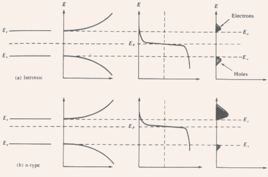
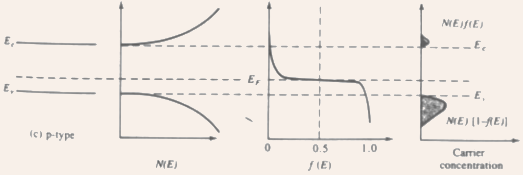
Fig.2.4 The density of states N(E), the Fermi-Dirac distribution function f(E), and the carrier concentration as functions of energy for (a) intrinsic, (b) n-type, and (c) p-type semiconductors at thermal equilibrium.
- Note: since the function f(E) is symmetrical about
 ,
a large electron concentration implies a small hole concentration,
and vice versa.
,
a large electron concentration implies a small hole concentration,
and vice versa.
- In n-type material, the electron concentration in the conduction
band increases as
moves closer to
 ; thus, (
-)
gives a measure of n.
; thus, (
-)
gives a measure of n.
- Similarly, in p-type material, the hole concentration in the valence
band increases as
moves closer to
 ;
thus, (-)
gives a measure of p.
;
thus, (-)
gives a measure of p.