- In indirect materials, the probability of direct band-to-band recombination
is very small recombination in these materials proceed through the
assistance of recombination (or trapping) centers located within the
band gap, which trap carriers of one type followed by trapping carriers
of the opposite type, thus annihilating the pairs.
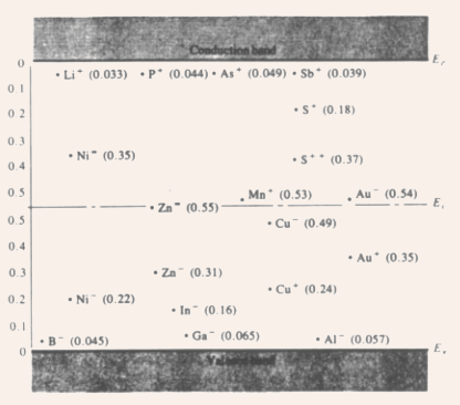
Fig.3.3 Energy levels of common impurities in silicon, measured from the closest band edge.
- The resulting energy loss is often in the form of heat given to
the lattice (instead of light emission), and, thus, these materials
are not well suited for optoelectronic applications.
- There are four probabilities associated with a recombination center:
(a) hole capture: when an electron from the recombination center falls to the valence band,
(b) hole emission: when an electron makes a transition from the valence band to the recombination center,
(c) electron capture: when an electron falls from the conduction band to the recombination center, and
(d) electron emission: when an electron makes a transition from the recombination center to the conduction band.
- Each of these processes has their own probabilities and time constants,
and the resulting analysis is significantly complicated.
- This theory of recombination is known as the SHR (Shockley-Hall-Read)
theory of recombination.
- If process (a) follows process (c) or vice versa, recombination
takes place, whereas, if process (b) follows process (a) (or vice
versa) or process (c) follows process (d) (or vice versa), it is known
as reemission, and the recombination center behaves like a trapping
center.
- Generally, centers that are located towards the middle of the band
gap (e.g., Au in Si) behave like recombination centers, whereas centers
located closer to the conduction or valence band behave as traps,
for obvious reasons.
- Alternate definition: in a center located within the band gap, if
after capturing one type of carrier, the most probable next event
is the capture of opposite type of carrier, then it is a recombination
center, however, if the most probable next event is reexcitation,
then it is a trap.
- The recombination can be slow or fast, depending on the amount of
time the carrier spends in the center before the capture of the opposite
type of carrier happens, thus, computation of lifetime for this kind
of indirect recombination is sufficiently complicated.
- The decay of excess carriers can be measured by a typical photoconductive decay measurement, where light shining on a sample is suddenly switched off, and the resulting decay of current passing through the sample is measured, the rate of decay of this current gives the excess carrier lifetime.
- Note: the lifetime is proportional to the inverse of the doping
concentration.
- However, at relatively high doping levels, the lifetime decreases
at a faster rate with an increase in the doping concentration.
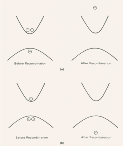
- This is because a different recombination mechanism, called the
Auger recombination becomes dominant at high doping levels.
- In this recombination mechanism, the electron and hole recombine
without involving trap levels, and the released energy (of the order
of the energy gap) is transferred to another carrier (a hole in p-type
material and an electron in n-type material).
- This process is somewhat the inverse of the impact ionization process,
in which an energetic carrier causes EHP generation.
- Since two electrons (in n-type material) or two holes (in p-type
material) are involved in this process, it is highly unlikely except
in heavily doped material.
- The recombination lifetime associated with the Auger recombination
process is inversely proportional to the square of the majority carrier
concentration, i.e., for p-type material,
 , and for n-type material,
  ,
where Gp and Gn are coefficients with values of
,
where Gp and Gn are coefficients with values of  and
and  .
.
![]() Surface
Recombination
Surface
Recombination
- It is obvious that near the surface of any semiconductor device,
the carrier recombination rate should be very high, due to extra defects
and traps at the surface.
- Thus, the diffusion flux of minority carriers at the surface is determined by the surface recombination processes.
- For example, when minority carriers are holes, this surface recombination
can be described by:
- where x = 0 corresponds to the surface of the sample, and
 is the surface recombination rate, with
  being the capture cross-section for holes,
  is the thermal velocity for the holes, and
  is the surface density of the surface states.
- The capture cross-section (typically
 )
describes the effectiveness of the localized state in capturing a
carrier.
)
describes the effectiveness of the localized state in capturing a
carrier.
- The product
may be visualized as the volume swept out per unit time by a particle
with cross-section

- If the surface state lies within this volume around the carrier,
then the carrier gets captured by the surface state.
- Note: the dimension of S is cm/sec, and, consequently, it is termed
as the surface recombination velocity, even though it has nothing
to do with actual velocity.
Fig.3.4 Auger recombination: (a) n-type sample, and (b) p-type sample.
![]() Steady State Carrier Generation: Quasi-Fermi Levels
Steady State Carrier Generation: Quasi-Fermi Levels
- For any temperature T, there is a thermal generation rate g(T) balanced
by a recombination rate r(T).
- Now, if a steady light is shone on the sample, an optical generation
rate
 will
be added to g(T), and the carrier concentrations n and p would increase
to their new steady state values.
will
be added to g(T), and the carrier concentrations n and p would increase
to their new steady state values.
- Generation/recombination rate balance equation:

- For steady state recombination and no trapping,
 ;
and, under low level injection approximation
;
and, under low level injection approximation

- Thus, the excess carrier concentrations can be given by

- In general, when trapping is present,
 ,
and
,
and  and
and  .
.
- Note: when excess carriers are present,
 .
.
- When excess carriers are present, the equilibrium Fermi level
 is
no more meaningful; instead, the carrier concentrations are defined
in terms of quasi-Fermi levels (also referred to as Imref, which is
Fermi spelled backwards)
is
no more meaningful; instead, the carrier concentrations are defined
in terms of quasi-Fermi levels (also referred to as Imref, which is
Fermi spelled backwards)  as
as

- Imref for the minority carriers deviates significantly from the
equilibrium Fermi level, whereas, for majority carriers, the Imref
stays very close to the equilibrium Fermi level, and the separation
between these two Imrefs is a measure of how far the system is from
equilibrium.
- With concentrations varying with position, the Imrefs would also vary with position, thus drawing Imrefs in band diagrams clearly shows the positional variations of the carrier concentrations.
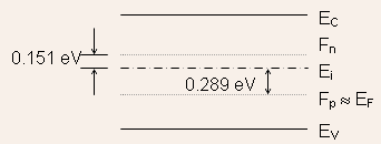
EXAMPLE 3.2
A Si sample with
is illuminated by a steady light thus creating
optically. Assume no trapping, and
(a) Determine the electron and hole concentrations n and p respectively, and their percentage change from the equilibrium concentrations.
(b) Comment on the magnitude of the product np.
(c) Determine the locations of the Imrefs,and compare their locations with the equilibrium Fermi leve
SOLUTION
(a) The equilibrium hole concentration
Since there is no trapping and
,therefore, the excess electron and hole concentrations can be given by
Therefore, the net electron concentration is given by
and the net hole concentration is given by
Therefore, the percentage change in the electron concentration
And the percentage change in the hole concentration
Note: with optical excitation (under the low-level injection approximation), there is a very large change in the minority carrier concentration, whereas the change in the majority carrier concentration is hardly noticeable!
(b) Note:
Whenever excess carriers are present,
(c) In equilibrium,
In the presence of excess carriers, the electron Imref
and the hole Imref
Thus, the majority carrier Imref almost coincides with the equilibrium Fermi level, whereas the minority carrier Imref shows a large departure from the equilibrium value.
![]() Photoconductive Devices
Photoconductive Devices
- Devices which change their resistance while exposed to light.
- Examples: automatic night light controllers, exposure meters in
cameras, moving-object counters, burglar alarms, detectors in fiber
optic communication systems, etc.
- Considerations in choosing a photoconductor for a given application:
sensitive wavelength range, time response, and optical sensitivity
(responsivity) of the material.
- The photoconductivity change while exposed to light is

- Obvious that for large changes in
 ,
the carrier mobility and lifetime should be high (e.g., in
,
the carrier mobility and lifetime should be high (e.g., in 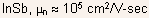 ,
and could be used as infrared detector with high sensitivity).
,
and could be used as infrared detector with high sensitivity).
- Time response is limited by recombination times, degree of carrier
trapping, and time required for the carriers to drift through the
device in an electric field.
- Dark resistance (i.e., the resistance of the device without any
illumination) should be as small as possible.
- Generally, all these requirements cannot be satisfied simultaneously, and some kind of optimization is required.
![]() Diffusion of Carriers
Diffusion of Carriers
- When excess carriers are created in a semiconductor and their concentrations
vary with position, then there is a net carrier motion from regions
of higher concentration to regions of lower concentration.
- This type of motion is called the diffusion, and it is an important
charge transport mechanism in semiconductors.
- Diffusion and drift are the two main current transport mechanisms.
![]() Diffusion processes
Diffusion processes
- Natural result of the random motion of individual electrons.
- Electrons move randomly and experience collisions, on the average,
after each mean free time .
- Since the motion is truly random, an electron has equal probability of moving into or out of a volume through a boundary.
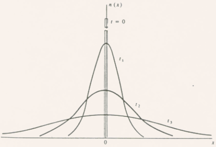
- A pulse of excess electrons injected at x = 0 at time t = 0 will spread out in time due to diffusion, and eventually n(x) becomes a constant, when no more net motion takes place.
Fig.3.5 Spreading of a narrow pulse of electrons created at x = 0 at t = 0 with time