- Electrons are restricted to sets of discrete energy levels within
atoms, with large gaps among them where no energy state is available
for the electron to occupy.
- Electrons in solids also are restricted to certain energies and are
not allowed at other energies.
- Difference
 in the solid, the electron has a range (or band) of available
energies.
in the solid, the electron has a range (or band) of available
energies.
- The discrete energy levels of the isolated atom spread into bands
of energies in the solid because
i) in the solid, the wave functions of electrons in neighboring atoms overlap, thus, it affects the potential energy term and the boundary conditions in the equation, and different energies are obtained in the solution, and
ii) an electron is not necessarily localized at a particular atom.
- The influence of neighboring atoms on the energy levels of a particular atom can be treated as a small perturbation, giving rise to shifting and splitting of energy states into energy bands.
Bonding Forces in Solids
![]() Ionic
Bonding
Ionic
Bonding
- Example: NaCl.
- Na (Z = 11) gives up its outermost shell electron to Cl (Z=17) atom,
thus the crystal is made up of ions with the electronic structures of
the inert atoms Ne and Ar.
- Note: the ions have net electric charges after the electron exchange
 ion
has a net positive charge, having lost an electron, and
ion
has a net positive charge, having lost an electron, and  ion
has a net negative charge, having acquired an electron.
ion
has a net negative charge, having acquired an electron.
- Thus, an electrostatic attractive force is established, and the balance
is reached when this equals the net repulsive force.
- Note: all the electrons are tightly bound to the atom.
- Since there are no loosely bound electrons to participate in current
flow
NaCl is a good insulator.
- In metals, the outer shell is filled by no more than three electrons
(loosely bound and given up easily)
 great
chemical activity and high electrical conductivity.
great
chemical activity and high electrical conductivity.
- Outer electron(s) contributed to the crystal as a whole
solid made up of ions with closed shells immersed in a sea of free electrons,
which are free to move about the crystal under the influence of an electric
field.
- Coulomb attraction force between the ions and the electrons hold the lattice together.
- Exhibited by the diamond lattice semiconductors.
- Each atom surrounded by four nearest neighbors, each having four electrons
in the outermost orbit.
- Each atom shares its valence electrons with its four nearest neighbors.
- Bonding forces arise from a quantum mechanical interaction between
the shared electrons.
- Both electrons belong to each bond, are indistinguishable, and have
opposite spins.
- No free electrons available at 0 K, however, by thermal or optical
excitation, electrons can be excited out of a covalent bond and can
participate in current conductionimportant
feature of semiconductors.
- Shown by III-V compounds bonding partly ionic and partly covalent.
- Ionic character of bonding becomes more prominent as the constituent atoms move further away in the periodic table, e.g., II-VI compounds.
- As isolated atoms are brought together to form a solid, the electron
wave functions begin to overlap.
- Various interactions occur, and, at the proper interatomic spacing
for the crystal, the forces of attraction and repulsion find a balance.
- Due to Pauli exclusion principle, the discrete energy levels of individual
atoms split into bands belonging to the pair instead of to individual
atoms.
- In a solid, due to large number of atoms, the split energy levels for essentially continuous bands of energy.
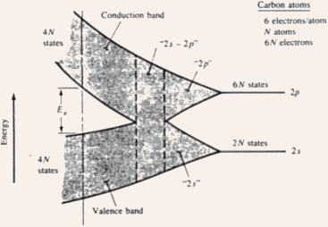
Fig.2.1 Splitting of individual energy levels to energy bands as atoms are brought closer together.
- Imaginary formation of a diamond crystal from isolated carbon atoms
 .
.
- Each atom has two 1s states, two 2s states, six 2p states, and higher
states.
- For N atoms, the numbers of states are 2N, 2N, and 6N of type 1s,
2s, and 2p respectively.
- With a reduction in the interatomic spacing, these energy levels split
into bands, and the 2s and 2p bands merge into a single band having
8N available states.
- As the interatomic spacing approaches the equilibrium spacing of diamond
crystal, this band splits into two bands separated by an energy gap
 ,
where no allowed energy states for electrons exist
forbidden gap.
,
where no allowed energy states for electrons exist
forbidden gap.
- The upper band (called the conduction band) and the lower band
(called the valence band) contain 4N states each.
- The lower 1s band is filled with 2N electrons, however, the 4N electrons
residing in the original n = 2 state will now occupy states either in
the valence band or in the conduction band.
- At 0 K, the electrons will occupy the lowest energy states available
to them
thus, the 4N states in the valence band will be completely filled, and
the 4N states in the conduction band will be completely empty.
- For electrons to move under an applied electric field, there must
be states available to them.
- A completely filled band cannot contribute to current transport; neither
can a completely empty band.
- Thus, semiconductors at 0 K are perfect insulators.
- With thermal or optical excitation, some of these electrons can be
excited from the valence band to the conduction band, and then they
can contribute to the current transport process.
- At temperatures other than 0 K, the magnitude of the band gap separates
an insulator from a semiconductor, e.g., at 300 K, (diamond)
= 5 eV (insulator), and
(Silicon) = 1.12 eV (semiconductor).
- Number of electrons available for conduction can be increased greatly
in semiconductors by reasonable amount of thermal or optical energy.
- In metals, the bands are either partially filled or they overlap thus,
electrons and empty states coexist
great electrical conductivity.
- In a typical quantitative calculation of band structures, the wave
function of a single electron traveling through a perfectly periodic
lattice is assumed to be in the form of a plane wave moving in the x-direction
(say) with propagation constant k, also called a wave vector.
- In quantum mechanics, the electron momentum can be given by

- The space dependent wave function for the electron is
 (2.1)
(2.1)
where the function modulates the wave function according to the periodicity of the lattice.
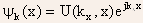
- Allowed values of energy, while plotted as a function of k, gives
the E-k diagram.
- Since the periodicity of most lattices is different in various directions, the E-k diagram is a complex surface, which is to be visualized in three dimensions.
Fig.2.2 Direct and indirect transition of electrons from the conduction band to the valence band: (a) direct - with accompanying photon emission, (b) indirect via defect level.
- Direct band gap semiconductor: the minima of the conduction band and
the maxima of the valence band occur at the same value of kan
electron making the smallest energy transition from the conduction band
to the valence band can do so without a change in k (and, the momentum).
- Indirect band gap semiconductor: the minima of the conduction band
and the maxima of the valence band occur for different values of k,
thus, the smallest energy transition for an electron requires a change
in momentum.
- Electron falling from conduction band to an empty state in valence
band recombination.
- Recombination probability for direct band gap semiconductors is much
higher than that for indirect band gap semiconductors.
- Direct band gap semiconductors give up the energy released during
this transition (= )
in the form of light used
for optoelectronic applications (e.g., LEDs and LASERs).
- Recombination in indirect band gap semiconductors occurs through some defect states within the band gap, and the energy is released in the form of heat given to the lattice.
- The band structures of III-V ternary and quaternary compounds change
as their composition is varied.
- There are three valleys in the conduction band:
 (at k = 0), L, and X.
- In GaAs, the
valley has the minimum energy (direct with =
1.43 eV) with very few electrons residing in L and X valleys (except
for high field excitations).
- In AlAs, the X valley has minimum energy (indirect with
= 2.16 eV).
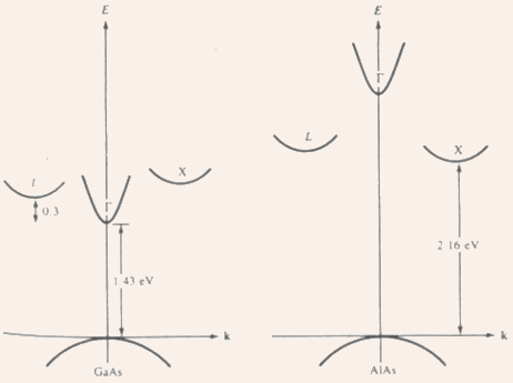
Fig.2.3 The E-k diagram of (a) GaAs and (b) AlAs, showing the three valleys (L,
- In a metal, the atoms are imbedded in a "sea" of free electrons,
and these electrons can move as a group under the influence of an applied
electric field.
- In semiconductors at 0 K, all states in the valence band are full,
and all states in the conduction band are empty.
- At T > 0 K, electrons get thermally excited from the valence band
to the conduction band, and contribute to the conduction process in
the conduction band.
- The empty states left in the valence band can also contribute to current
conduction.
- Also, introduction of impurities has an important effect on the availability
of the charge carriers.
- Considerable flexibility in controlling the electrical properties of semiconductors.
- For T> 0 K, there would be some electrons in the otherwise empty
conduction band, and some empty states in the otherwise filled valence
band.
- The empty states in the valence band are referred to as holes.
- If the conduction band electron and the valence band hole are created
by thermal excitation of a valence band electron to the conduction band,
then they are called electron-hole pair (EHP).
- After excitation to the conduction band, an electron is surrounded
by a large number of empty states, e.g., the equilibrium number of EHPs
at 300 K in Si is
 ,
whereas the Si atom density is
,
whereas the Si atom density is .
.