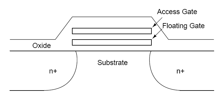
Over the years, various attempts have been made to create a device with electrically alterable characteristics and enough reliability to support a multitude of write cycles. For example, the MNOS(Metal Nitride Oxide Semiconductor) transistor held promise, but has been unsuccessful until now. In this device, threshold-modifying electrons are trapped in a layer deposited on the top of the gate . A more accepted solution is offered by the floating gate transistor shown in Figure 32.21, which forms the core of virtually every NVRW memory built today.
Fig 32.21: FAMOS Structure
The structure is similar to traditional MOS device, except that an extra polysilicon strip is inserted between the gate and channel. This strip is not connected to anything and is called as Floating gate. The most obvious impact of inserting this extra gate is to double the gate oxide thickness , which results in a reduced device transconductance as well as increased threshold voltage. Both these properties are not particularly desirable.
This device has property that its threshold voltage is programmable. Applying a high voltage (about 10V) between the source and drain terminals creates a high electric field and causes avalanche injection to occur. Electrons acquire sufficient energy to become 'HOT' and traverse through the first oxide insulator, so that they get trapped on the floating gate. This phenomenon can occur with oxide as thick as 100nm, which makes it relatively easy to fabricate the device. In reference to the programming mechanism, the floating gate transistor is often called Floating Gate Avalanche Injection MOS (FAMOS).
The trapping of electrons on the floating gate effectively drops the voltage on that gate. This process is self-limiting and the negative charge accumulated on the floating gate reduces the electrical field over the oxide so that ultimately it becomes incapable of accelerating more hot electrons. Removing the voltage leaves the induced negative charge in place, and results in a negative voltage on the intermediate gate. From the device point of view, this translates into an effective increase in threshold voltage. To turn on the device, a higher voltage is needed to overcome the effect of the induced negative charge. Typically, the resulting threshold voltage is around 7V; thus a 5V gate-to-source voltage is not sufficient to turn on the transistor, and the device is effectively disabled.
Since the floating gate is surrounded by , which is an excellent insulator, the trapped charge can be stored for many years, even when the supply voltage is removed, creating the nonvolatile storage mechanism. One of the major concerns of the floating gate approach is the need for high programming voltages. By tailoring the impurity profiles, technologists have been able to reduce the required voltage from the original 25V to approximately 12.5V in today's memories.