Lecture 22 : Logical Effort Calculation of few Basic Logic Circuits
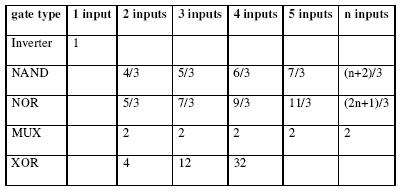
22.7 Tabular View of Logical Efforts
Logical effort for different circuits is tabulated in the table below in fig. 22.71
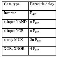
The parasitic delays for different is tabulated in fig. 22.72.
Now delay, d = gh+ p
For example, dINV = (1*1) +1=2.
If we assume tau = 25 ps
Absolute delay dABS =50 ps.
Fig 22.71: Logical efforts of basic gates with different input configurations
Fig 22.72: parasitic delay of basic gates
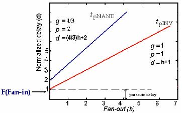
22.8 Delay Plot
The delay of a simple logic gate as represented in equation d = gh + p is a simple linear relationship. The fig 22.8 shows this
relationship graphically. Delay appears as
a function of electrical effort for an inverter and for a two-input NAND gate.The slope of
each line is the logical effort of the gate.It’s intercept is the parasitic delay. The graph shows that we can adjust the total delay by adjusting the electrical effort or by choosing a logic gate with a different logical effort.
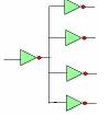
Example3: Fonout-of-4 (FO4) inverter circuit- Because each inverter is identical, Cout = 4Cin, so h = 4. The logical effort g = 1 for an invreter.Thus FO4 delay is,
d = gh + p = 1*4 + pINV =4 + 1 = 5.