Module 4 : Propagation Delays in MOS
Lecture 22 : Logical Effort Calculation of few Basic Logic Circuits
 
22.3 Logical Effort of a NAND Gate
A NAND gate contain two NMOS (pull down) transistors in series and two PMOS (pull up)transistors as shown in fig 22.3).

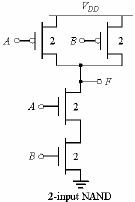
We have to size the transistors such that the gate has the same drive characteristics as an inverter with a pull down of width 1 and a pull up of width 2. Because the two pull down transistors are in series, each must have the twice the conductance of the inverter pull down transistor so that the series connection has a conductance equal to that of the inverter pull down transistor. Hence these two transistors should have twice the width compared to inverter pull down transistor. By contrast, each of the two pull up transistors in parallel need be only as large as the inverter pull up transistor to achieve the same drive as the reference inverter. So, the logical effort per input can be calculated as
g = (2+2)/ (1+2) = 4/3.
For 3 input NAND gate, g = (3+2)/ (1+2) =5/3
For n input NAND gate, g = (n+2)/ 3

Fig 22.3:2-input NAND  
 
22.4 Logical Effort of a NOR Gate
A NOR gate contain two pull down transistors in parallel and two pull up transistors in series as shown in figure 22.4.
Because the two pull up transistors are in series, each must have the twice the conductance of the inverter pull up transistor so that the series connection has a conductance equal to that of the inverter pull up transistor. Hence these two transistors should have twice the width compared to inverter pull down transistor. By contrast, each of the two pull down transistors in parallel need be only as large as the inverter pull down transistor to achieve the same drive as the reference inverter. So, the logical effort per input can be calculated as-
effort of NOR gate, g = (1+4)/ (1+2) = 5/3
For n input NOR gate, g = (2n+1)/3
Fig 22.4: 2-input NOR


3