17.3 |
CMOS Summary
|
| |
Logic consumes no static power in CMOS design style.
However, signals have to be routed to the n pull down network as well as to the p pull up network.
So the load presented to every driver is high.
This is exacerbated by the fact that n and p channel transistors cannot be placed close together as these are in different wells which have to be kept well separated in order to avoid latchup.
|
| |
 |
 |
17.4 |
Pseudo nMOS Design Style
|
| |
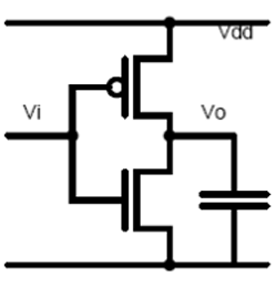
The CMOS pull up network is replaced by a single pMOS transistor with its gate grounded.
Since the pMOS is not driven by signals, it is always on'.
The effective gate voltage seen by the pMOS transistor is Vdd. Thus the overvoltage on the p channel gate is always Vdd -VTp.
When the nMOS is turned on', a direct path between supply and ground exists and static power will be drawn.
However, the dynamic power is reduced due to lower capacitive loading.
|
17.5 |
Static Characteristics |
| |
As we sweep the input voltage from ground to , we
encounter the following regimes of operation: |
|
nMOS ‘off’ |
|
nMOS saturated, pMOS linear |
|
nMOS linear, pMOS linear |
|
nMOS linear, pMOS saturated |
| |
|
|