Lecture 16 : Propagation Delay Calculation of CMOS Inverter
16.3 Rise and Fall Times
Figure 16.21 shows the familiar CMOS inverter with a capacity load CL that
represents the load capacitance (input of next gates, output of this gate and routing). Of interest is
the voltage waveform Vout(t) when the input is driven by a step waveform, Vin(t) as shown in
figure 16.22 .
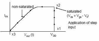
Figure 16.31 shows the trajectory of the n-transistor operating point as the input voltage, Vin(t), changes from 0V to VDD. Initially, the end-device is cutt-off and the load capacitor is charged to VDD. This illustrated by X1 on the characteristic curve. Application of a step voltage
(VGS=VDD) at the input of the inverter changes the operating point to X2. From there onwards
the trajectory moves on the VGS=VDD characteristic curve towards point X3 at the origin.
Fig 16.31: trjectory of n-transistor operating point
Thus it is evident that the fall time consists of two intervals;
1.tf1=period during which the capacitor voltage, Vout, drops from 0.9VDD to (VDD– Vtn)
2. tf2=period during which the capacitor voltage, Vout, drops from (VDD – Vtn ) to 0.1VDD.
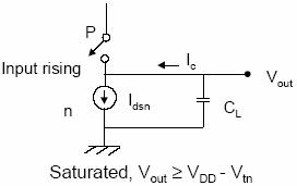
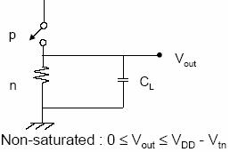
The equivalent circuits that illustrate the above behavior are show in figure (16.32 & 16.33 ).
Figure 16.32: Equivalent circuit for showing behav. of tf1
Figure 16.33: Equivalent circuit for showing behav. of tf2
As we saw in last section, the delay periods can be derived using the general equation