Lecture 16 : Propagation Delay Calculation of CMOS Inverter
16.1 Few Definitions
Before calculating the propagation delay of CMOS Inverter, we will define some basic terms-
• Switching speed - limited by time taken to charge and discharge, CL .
• Rise time, tr : waveform to rise from 10% to 90% of its steady state value
• Fall time tf, : 90% to 10% of steady state value
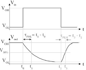
• Delay time, td : time difference between input transition (50%) and 50% output level
The propagation delay tp of a gate defines how quickly it responds to a change at its inputs, it expresses the delay experienced by a signal when passing through a gate. It is measured between the 50% transition points of the input and output waveforms as shown in the figure 16.1 for an inverting gate. The defines the response time of the gate for a low to high output transition, while refers to a high to low transition. The propagation delay as the average of the two