Semiconductors:
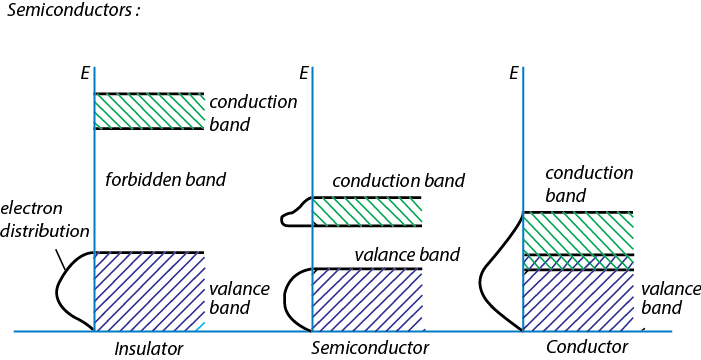
Figure 2.15. Schematic representation of band gap between valence band and conduction band in insulator, semiconductor and conductor are shown.
Semiconductors are solid materials where a small energy gap, known as band gap, is present between the valence electron-containing valence band and conduction band. If the system (semiconductor) is cooled to absolute zero, the electrons will occupy the lowest possible energy according to the Boltzmann´s distribution law. Hence, the valence band will be full of electron, while, conduction band will not occupy any free electron for conduction. Therefore, this system is said to be an insulator. With increase of temperature some of electrons will occupy conduction band. Hence, an electric conduction can take place by passing electrons.
Example: Germanium (Ge) and silicon (Si) are mostly used semiconductors and will be discussed here.
Both of them have diamond-like structure. Both of them are tetravalent, i.e. contains four electrons in the outermost shell which forms four covalent bonds with the other atoms. Both of them at very low temperature behave as an insulator. The band gap for Ge is 68 kJmol−1 and for Si it is 106 kJmol−1 . Therefore, even at room temperature they are almost insulators. When they are connected to a electric circuit in the room temperature they are slightly conducting. This is known as intrinsic semiconduction. As the temperature increases conduction increases due to promotion of valence electrons to the conduction band.
n -Type and p -type semiconductors:
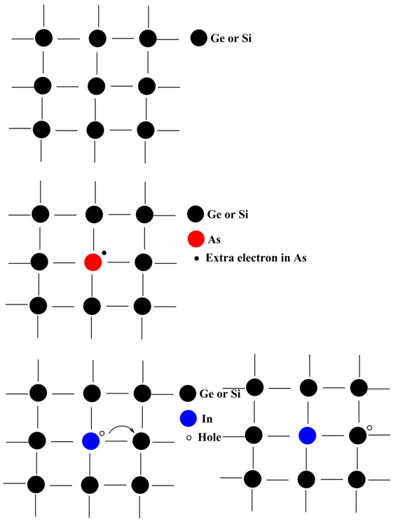
Figure 2.16. Pure lattice (top), n-type semiconductor (middle), p-type semiconductor (bottom)