Introduction: We start with some information on the importance of the BEOL processes. Then we will consider the metal choice of Al vs Cu as interconnect. Using these as examples, we will learn about the best way to combine different processes to achieve the goal of a robust process sequence. Integration literally means ‘unification’ or ‘putting together many things’. Here process integration means matching or combining different processes to obtain a finally ’passing’ or good chip. The ultimate purpose is to make the process robust so that many chips can be produced with maximum number of chips in good condition at the minimum cost.
Importance of BEOL: In the FEOL section, we learnt that the speed of a particular transistor is controlled by the gate length. Hence, when the size of the transistors decreased, the gate length decreased and the transistor speed increased. As an example, computers with 100 MHz speed were commercially available around 1995, and the speed continued to increase until it reached around 3 GHz. This is because with improvement in technology, it is possible to make transistors of smaller size. After about 3 GHz, a further increase in speed is not seen, at least in the commercially available chips. However, more ‘cores’ are made in a single chip and the functionality improves without an increase in speed. Why?
The transistors in the newer chips are smaller than the transistors of older chips. Thus the transistors can be switched on or off more quickly. But the signal from one transistor to another goes through the metal wires and the time delay is more in the newer chips. The delay is related to the resistance of the metal wire and the capacitance between the metal wires. This is also called as “RC delay”. (See Fig. 9.1)
When the transistors are made small, the connecting wires are also made small, which increases the metal resistance. When many transistors are packed closely in a chip, the metal wires connecting them also run close to each other. Thus the capacitance between the metal wires increases. This increases RC delay. Originally aluminum was used as interconnect and SiO2 was used as the insulator between the metal lines. The metal resistance can be decreased by replacing aluminum with copper. The capacitance can be decreased by replacing SiO2 with other materials with low-dielectric constant.
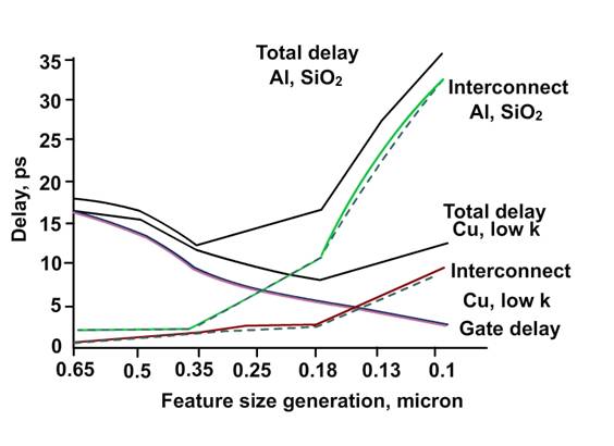
Fig 9.1. A qualitative plot illustrating the estimates of delay vs feature size. Notice that the feature size decreases along the abscissa (“X-axis”).
The transistors made in one layer, whereas the metal lines connecting them are made in many layers (~ 9 layers in some chips in 2011). The connections between the transistors are so complex that they can not be made in less number of layers. While making the transistors needs a complex sequence of processes, making a layer of interconnect is relatively less complex. As an example, the yield (i.e. success rate) of FEOL may be 95% . The yield of a single layer of interconnect (i.e .part of BEOL) may be 98%. But since there are 9 layers of BEOL, if we assume that each layer has a yield of 98%, the total BEOL yield is approximately (0.98)9 = 83%. Thus for the most modern chips, the BEOL part of the chip (i.e. interconnects and insulators) determine the speed of the chip and play a significant role in affecting the yield of the chip.
Marginal process vs robust process: A process is called marginal if a slight change in any of the conditions causes the process to change drastically. In contrast, a process is robust if it gives proper results even if there are minor changes in the conditions.
Aluminum process: When aluminum is used as interconnect material, a layer of titanium and titanium nitride is used as a barrier and adhesion promoter. This prevents the diffusion of aluminum atoms through the insulator. The insulator material used is SiO2. The sequence of process steps needed to fabricate a via and a metal line are given below.
Let us assume that the fabrication of M1 is completed and that via12 and M2 have to be fabricated. i.e. the chip is at the stage as shown in Fig.9. 2(a) and we need to process it so that it becomes as shown in Fig 9. 2(b).
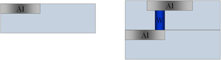
Fig 9.2. Schematic of chip in BEOL (a) after M1 layer (b) after fabrication of via12 and M2 layer
First, a layer of silicon dioxide is deposited on top of M1 (Fig 9.3a). Then using lithography and plasma etching, via12 hole is made (Fig 9.3b). Next, a thin layer of TiN/Ti is deposited on top. This film is formed on the top of the surface as well as on the sides and bottom of the via hole (Fig 9.3c). Then, W is deposited using CVD (Fig 9.3d). Excess W is removed using CMP (Fig 9.3e).
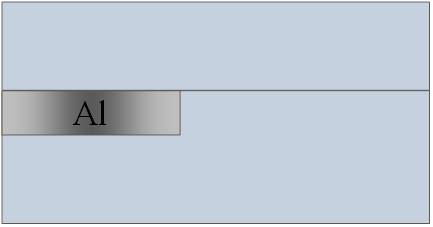
Fig. 9.3(a) Deposition of insulator (silicon dioxide)
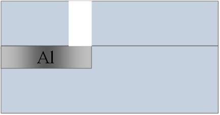
Fig. 9. 3(b) Lithography and dry etching (plasma etching) to create via hole
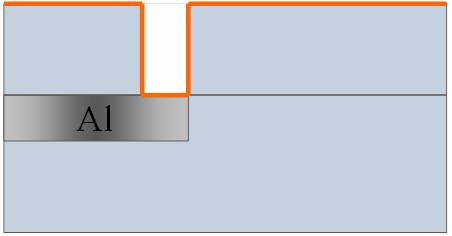
Fig. 9. 3(c), Ti/TiN liner deposition by PVD
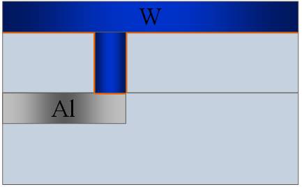
Fig. 9.3(d), Tungsten deposition by CVD
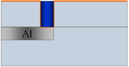
Fig. 9. 3(e) Removal of excess tungsten by CMP
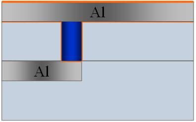
Fig. 9. 3(f) Deposition of aluminum and Ti/TiN liner by PVD
In the next step, aluminum and titanium are deposited on the top. After that, using lithography and plasma etching, aluminum is removed from unwanted locations. The titanium barrier layer is also removed along with aluminum in those locations.
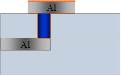
Fig. 9. 3(g) Lithography and dry etching to remove excess aluminum and Ti/TiN liner
Fig. 9. 3(h) Deposition of insulator (silicon dioxide) by CVD
Oxide layer is deposited on top of the aluminum and the non-planar surface is subjected to CMP, to make it planar. This is necessary so that subsequently lithography can be done on the surface with minimal distortions.
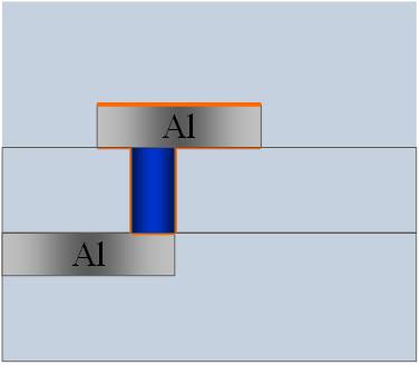
Fig. 9. 3(i) Planarization of the insulator layer by CMP
ESD and Antenna effect: Electrostatic discharge (ESD) is a phenomenon of importance in aluminum plasma
etching. When charge builds up in a material, it is called static charge. It is usually found in insulators. As an example, if a glass rod is rubbed against a woolen cloth, it will build up static charge. It also varies with the environment: in humid atmospheres, the charge build up is low, whereas in dry environments, the charge build up is high. After rubbing the glass rod against wool, if the glass rod is brought near a metal, then the excess charge be discharged and a spark may be seen.
During aluminum etching, plasma is used and the presence of electrons and ions in the plasma causes the aluminum surface to be charged. Since aluminum is a conductor, the charge density is usually not high when the entire surface is exposed to plasma. However, sometime during etching, aluminum lines begin to be separated and finally when the etching is completed, many short metal lines and a few long metal lines would be formed.
We notice that the aluminum lines are connected to transistors and diodes. If too much charge builds up in the aluminum, then the diode or transistor may breakdown. This unwanted phenomenon is called ESD in IC manufacturing. If the metal lines are long, then they act as an antenna and collect more charge. This is called antenna effect. To minimize the problems due to this, during the design stage itself, the maximum length of the metal line will be limited. Similarly, in the design stage, a few diodes with certain specific characteristics will be added to the circuits so that if ESD occurs, then only those diodes will break down. These are sacrificial diodes and are sometimes called as ESD protection diodes. They are not part of the actual functioning of the chip and are present only to protect other transistors and diodes during the metal etching by plasma.
|