Normally, a few wafers will be etched for various times (e.g. 60 seconds, 90 seconds, 120 seconds etc) and the average removal rate would have been calculated based on those. From these values, the etching tool can be operated for a specific time so that the material can be removed up to the desired depth. Even then, there might be some variation in the etching and hence usually the tool is operated for at least 10% longer than the estimate. This is called “over etch”.
If the etching is continued for 10% more time, then won’t it remove the copper at the bottom? Yes, it will. In order to prevent it, there would be a silicon nitride layer on top of copper and below the silicon dioxide, as shown in figure 4.7. The silicon nitride layer will not be easily removed by the chemicals used in silicon dioxide etching. Hence 10% over etch of silicon dioxide will not remove the silicon nitride. After silicon dioxide is etched, the silicon nitride will be etched using dry etching, with different chemicals. Since the silicon nitride layer thickness is very small, the etching time is also very small and it can be etched with good control. Hence the problems due to under etch or over etch will not be there.
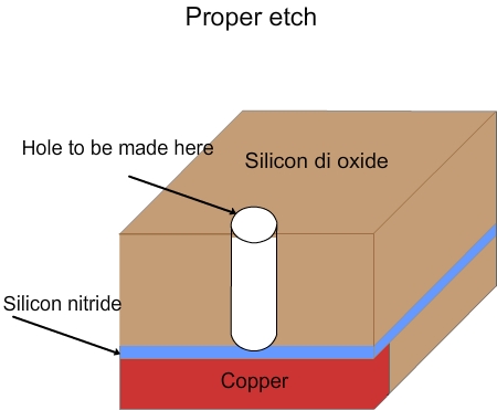
Figure 4.7. Schematic of proper etch using nitride layer in the process flow
Veil and de-veiling: In dry etching, the unidirectional etching is achieved due to two reasons. Since the plasma reacts with the material, heat will be generated. The photo resist will soften a bit and flow down. The flowing film will react with the plasma and form a hard layer, called veil. The veil will not react further with the plasma and will protect the side walls (Figure 4.8 a , b and c). After the completion of etching, the veil has to be removed by using different chemicals, by either wet etching or dry etching. The process of removing the veil is called de-veiling.
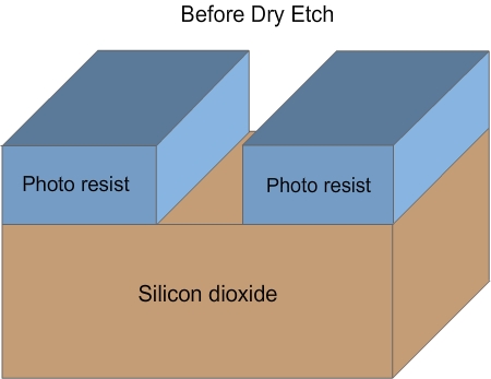
Figure 4.8 a. Schematic of wafer before dry etch
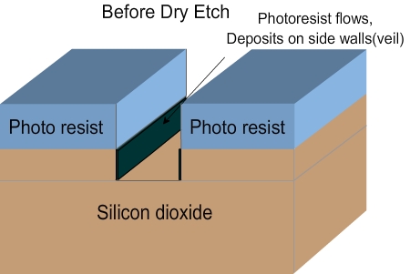
Figure 4.8 b. Schematic of veil formation during dry etch
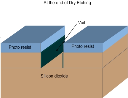
Figure 4.8 c. Schematic of the wafer at the end of dry etch. Note that the veil formation helps in anisotropic etch.
Secondly, the wafer is usually kept near the negative plate which is used for generating the plasma. The positive ions in the plasma will come towards the wafer and sputter away some material. Hence the etching will be unidirectional. This sputtering based removal can be enhanced by adding argon gas. Argon ions will attack the wafer and remove the material (Figure 4.9). However, they will not react with the wafer. The only disadvantage is that argon will attack both the material to be removed (like silicon dioxide) and the photo resist. The other chemicals in the plasma like CF4, H2, O2 can be changed and the removal of silicon or silicon dioxide can be controlled well. But the argon will remove all materials and the selectivity will be lowered. The dry etch without argon is called plasma etching and the one with argon is sometimes called reactive ion etching (RIE), since reacting chemicals as well as argon ions are present in that type of etching. By controlling the argon and other chemicals, it is possible to obtain very good anisotropic etching while maintaining acceptable selectivity.
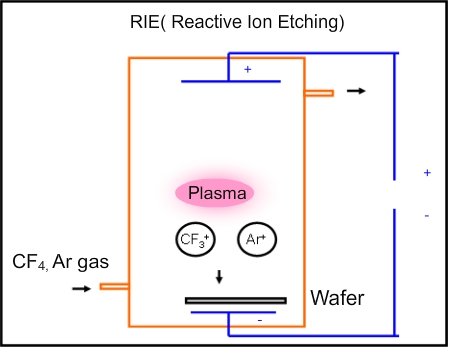
Figure 4.9. Schematic of Reactive Ion Etcher
Using magnetic field, the plasma can be confined to a small region and the density of the plasma can be increased. This is referred to as “high density plasma”. High density plasma will increase the etch rate significantly.
It is not practical to use etching for removing excess copper. In wet etching, there is no control and anisotropic etch will be catastrophic. In dry etching, at moderate temperatures, the reaction products are not volatile and hence they do not come out of the wafer. Hence another technique called chemical mechanical planarization or CMP is used for making copper interconnects.
One of the difficulties encountered in dry etching is electrostatic discharge (ESD). When aluminum is used as interconnect material, dry etch is used to remove unwanted aluminum. In the beginning, a continuous layer of aluminum would be present. At later stages, since some aluminum will be etched, islands of aluminum will form and finally the correct structures would be left. In presence of high voltage used for plasma generation, the aluminum islands can acquired charge. They are connected to the transistors at the bottom and if the charge accumulated is high, they can break the gate oxide and destroy the transistor. This is an example of electrostatic discharge (ESD). The charge accumulated is proportional to the area that the aluminum network can form during the process (i.e. the area of any island). During the design phase itself, the maximum area of such island is specified. Since the islands or network act as an antenna during dry etching, this rule is sometimes called as “antenna rule”. To minimize the risk of ESD, certain diodes are used as ‘safety valves’. Note that these diodes do not play any role in the chip design and functioning and are there only to ensure that the process does not destroy the transistor.
|