Dry etching.
In dry etching, chemical reaction occurs between the material on the wafer and the gases. In this method, the products of the reaction must be gaseous. Otherwise, the product will remain on the wafer.
Gases can etch only a few materials in the normal state. However, if we create plasma in the etching chamber, the gas molecules will split into ions, atoms and radicals. These are highly reactive and will react with almost any material.
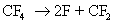
For example, if the silicon or silicon dioxide on top of the wafer has to be etched, carbon tetra fluoride ( ) and hydrogen ( ) and hydrogen ( ) gases can be used. The wafer will be held in an etching chamber, which also has plates with electrical connections. First the chamber will be evacuated and then and will be fed into the chamber at a slow rate (a few g/s). They will NOT react with silicon or silicon dioxide. If the plates are given high voltage, a plasma will form and this will split the gas molecules into ) gases can be used. The wafer will be held in an etching chamber, which also has plates with electrical connections. First the chamber will be evacuated and then and will be fed into the chamber at a slow rate (a few g/s). They will NOT react with silicon or silicon dioxide. If the plates are given high voltage, a plasma will form and this will split the gas molecules into  +, F, CF2+, H etc. These ions and radicals can react with silicon or silicon dioxide and etch them away. +, F, CF2+, H etc. These ions and radicals can react with silicon or silicon dioxide and etch them away.
An example of radical generation in presence of plasma is given below
The fluorine radicals and the  radicals generated are very reactive. They can react with silicon di oxide and form silicon tetra fluoride, which is a gaseous product. radicals generated are very reactive. They can react with silicon di oxide and form silicon tetra fluoride, which is a gaseous product.


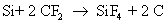
They also react with silicon to form silicon tetra fluoride

Note that carbon monoxide, carbon and oxygen radicals are also formed as byproducts. The actual number of reactions occurring during dry etch is very high, but only the main reactions are given here for the sake of simplicity. The reaction rate of silicon with fluoride ion is much more than the reaction rate of silicon dioxide with fluoride ion.
In presence of hydrogen, the fluorine radicals combine with hydrogen radicals as shown below.


This reduces the availability of fluorine radicals. If we want to remove silicon dioxide, but not silicon, then we have to send more of hydrogen and less of .
On the other hand, if in presence of oxygen, the availability of fluorine radicals will increase due to the following reaction


If we want to remove silicon and not silicon dioxide, we have to send and oxygen, instead of hydrogen. Thus it is possible to control the removal rate of silicon di oxide and silicon by suitably adjusting the feed gas concentrations.
Whatever may be the gas, if the voltage applied to the plates is removed, the plasma will disappear and the etching will stop. This is one major advantage of dry etching. We can start and stop the etching in a very short period of time. In case of wet etching, even if we take the wafer out of the bath, some of the chemicals will be on the surface of the wafer and will continue to etch the material until it is thoroughly washed and all the chemicals are removed.
One of the issues that can arise during etch is called microloading. Since the dry etch is conducted at low pressure, the concentration of reacting species will not be high. If a certain region has either a large trench or many small trenches, then that region will utilize most of the reactants in that area. Hence the etch rate will be normal in the beginning but will tend to decrease after some time. In other areas, where only small trenches need to be etched, only part of the reactants would be consumed at that time. Hence the etch rate will not decrease in those areas even after some time. Thus, there is a non uniformity in the average etch rate, depending on the ‘aerial density’ as viewed in the layout. This local variation in etch rate, due to the local depletion of reactants is called micro loading. In some fabs, while optical proximity correction (OPC) is implemented during mask making to account for the non-idealities in lithography, corrections are also implemented to account for micro loading. i.e. extra dummy structures may be used in areas with low aerial density so that the etch rate is uniform across the chip. This correction, accounting for the etch process and lithography, is called process proximity correction (PPC).
Under etch and over etch:
Let us consider an example to understand the dry etching used in IC manufacturing. Consider the schematic in fig 4.4. Here the copper wire at the bottom must be connected to the higher level. For that, the glass has to be etched at the right place. Then copper must be filled in the hole. We will consider only the etching part here. In the Figure 4.4, a hole needs to be etched or drilled through silicon dioxide, from the top in only one direction. It has to stop exactly at the copper level. If it etches less, it is ‘under etch’ and if it etches more, it is over etch. Both are problematic. If it etches in all directions, that is also a problem.
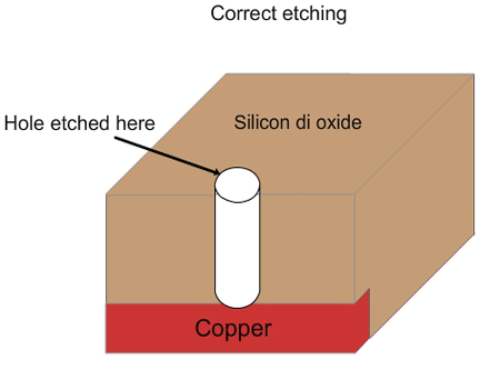
Figure 4.4. Example of correct etch.
In case of under etch, there will be some silicon dioxide left (Figure 4.5). Even if copper is deposited in the hole, it will not connect to the bottom copper line. So, the circuit won’t be complete and the IC will not work.
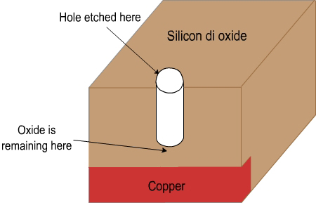
Figure 4.5. Schematic of under etch
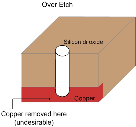
Figure 4.6. Schematic of over etch
In over etch, the copper line at the bottom will get corroded and may even completely disappear (Figure 4.6). This will also lead to the failure of the chip. Also, if the etching happens in all directions, there may be a problem that it will touch a neighboring contact. So, unidirectional etching is essential.
|