Atomic force microscopy is a member of the microscopic techniques together known as scanning probe microscopy (SPM). The working principle of scanning probe microscopes is very different from those underlying light and electron microscopy. An SPM is used to study the surface properties of materials by scanning a very fine pointed probe over the surface. SPM is a relatively new technique and emerged with the development of the first working SPM by Gerd Binnig and Heinrich Rohrer in 1981. The first SPM was a scanning tunneling microscope (Figure 19.1).
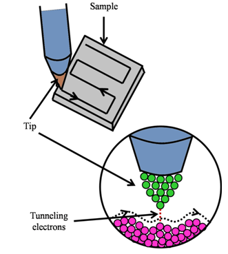
Figure 19.1 A schematic diagram of a scanning tunneling microscope.
The probe in a scanning tunneling microscope is a very fine metal tip at a high voltage. The tip is brought in a close proximity of the surface and scanned across the surface in a raster pattern. The quantity that is measured is the tunneling current flowing between the sample and the surface. The instrument can operate either in constant current mode or in constant height mode. In constant height mode, the tip scans the surface and current is recorded at each point. In a constant current mode, the current flowing between the tip and the sample is kept constant through a feedback loop that causes the sample stage to move closer to or farther from the tip; the signal obtained in constant current mode therefore is the distance between the tip and the specimen. An intrinsic limitation of scanning tunneling microscopy is its inability to study the non-conducting surfaces. This led to the development of other types of microscopes including atomic force microscope.