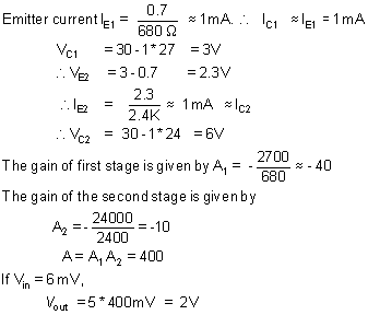
Direct Coupling:
For applications, where the signal frequency is below 10 Hz, coupling and bypass capacitors cannot be used. At low frequencies, these capacitors can no longer be treated as ac short circuits, since they offer very high impedance. If these capacitors are used then their values have to be extremely large e.g. to bypass a 100 ohm emitter resistor at 10 Hz, we need a capacitor of approximately 1600 m F. The lower the frequency the worse the problem becomes.
To avoid this, direct coupling is used. This means designing the stages without coupling and bypass capacitors, so that the direct current is coupled as well as alternating current. As a result, there is no lower frequency limit. The amplifier enlarges the signal no matter have low frequency including dc or zero frequency.
One Supply Circuit:
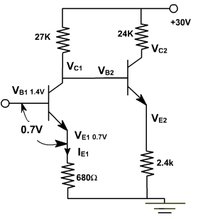
Fig. 8, shows a two stage direct coupled amplifier, no coupling or bypass capacitors are used. With a quiescent input voltage 1.4 V, emitter voltage = 1.4 - 0.7 = 0.7 V
The output varies from +6V to +8V.
Fig. 8
The main disadvantage is variation in transistor characteristic with variation in temperature. This causes IC and VC to change. Because of the direct coupling the voltage changes are coupled from one stage to next stage, appearing at the final output as an amplified voltage. The unwanted change is called drift.
Grounded Reference Input
For the above amplifier, we need a quiescent voltage of 1.4V. In most applications, it is necessary to have grounded reference input one where the quiescent input voltage is 0 V, as shown in fig. 9.
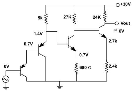
Fig. 9
The quiescent V CE of the first transistor is only 0.7V and the quiescent of the second transistor is only 1.4V. Both the transistors are operating in active region because VCE(sat) is only 0.1 volt. The input is only in mV, which means that these transistors continue to operate in the active region when a small signal is present.