Example- 3 (Capacitor-Coupled Emitter-Resistor Amplifier Design)
Design an emitter-resistor amplifier as shown in fig. 3 with AV =-10, β =200 and R load = 1K Ω. A pnp transistor is used and maximum symmetrical output swing is required.
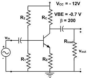
Fig. 3
Solution:
As designed earlier, we shall chose RC = Rload = 10 kΩ.
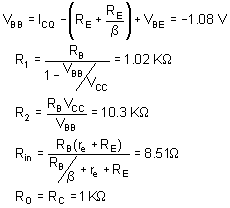
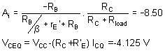
The voltage gain is given by
where R'E= RE + r'e.
Substituting AV, Rload and RC in this equation, we find R'E= 50 Ω.
We need to know the value of r'e to fine RE. We first find Rac and Rdc, and then calculate the Q point as follows (we assume r'e is small, so RE = R'E)
Rac = RE + RC || Rload = 550 Ω
Rdc = RE + RC = 1050 Ω
Now, the first step is to calculate the quiescent collector current needed to place the Q-point into the center of the ac load line (i.e., maximum swing). The equation is
The quantity, r'e , is found as follows
Then
RE = 50 - re = 46.67 Ω
If there were a current gain or input resistance specification for this design, we would use it to solve for the value of RB. Since is no such specification, we use the expression
RB =0.1 β RE = 0.1 (200) (46.6) = 932 Ω
Then continuing with the design steps,
and
The last equality assumes that rO is large compared to RC.
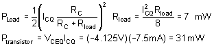
The maximum undistorted peak to peak output swing is given by
1.8 | ICQ | ( RC || Rload )=1.8 ( 0.0075 ) ( 500 ) = 6.75 V
The power delivered into the load and the maximum power dissipated by the transistor are found as
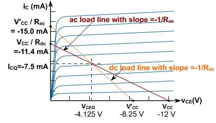
The load lines for this circuit are shown in fig. 4.
Fig. 4