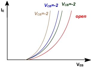
The Input Characteristic:
In the active region the input diode is forward biased, therefore, input characteristic is simply the forward biased characteristic of the emitter to base diode for various collector voltages. fig. 3. Below cut in voltage (0.7 or 0.3) the emitter current is very small. The curve with the collector open represents the forward biased emitter diode. Because of the early effect the emitter current increases for same VEB. (The diode becomes better diode).
When the collector is shorted to the base, the emitter current increases for a given VEB since the collector now removes minority carriers from the base, and hence base can attract more holes from the emitter. This mean that the curve VCB= 0, is shifted from the character when VCB = open.
Fig. 3
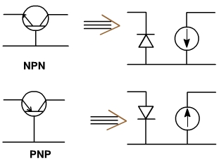
Equivalent circuit of a transistor: (Common Base)
In an ideal transistor, adc= 1. This means all emitter electrons entering the base region go on to the collector. Therefore, collector current equals emitter current. For transistor action, emitter diode acts like a forward bias diode and collector diode acts like a current source. The equivalent circuits of npn and pnp transistors are shown in fig. 4. The current source arrow points for conventional current. The current source is controlled by emitter current.
Fig. 4