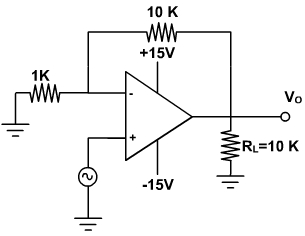
Example - 4
R1 = 100Ω, Rf = 8.2 k, RC = 10 k. Assume that the amplifier is nulled at 25°C. If Vin is 20 mV peak sine wave at 100 Hz. Calculate Er, and Vo values at 45°C for the circuit shown in fig. 2.
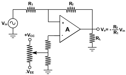
Fig. 2
Solution:
The change in temperature ΔT = 45 - 25 = 20°C.
Error voltage = 51.44 mV
Output voltage is 1640 mV peak ac signal which rides either on a +51.44 mV or -51.44 mV dc level.
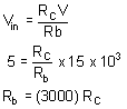
Example - 5
Design an input offset voltage compensating network for the operational amplifier µA 715 for the circuit shown in fig. 3. Draw the complete circuit diagram.
Fig. 3
Solution:
From data sheet we get vin = 5 mV for the operational amplifier µA 715.
V = | VCC | = | - VEE | = 15 V
Now,
If we select RC = 10Ω, the value of Rb should be
Rb = (3000) RC = 30000Ω = 304ΩSince R > Rmax, let RS = 10 Rmax where Rmax = Ra / 4. Therefore,
If a 124Ω potentiometer is not available, we may prefer to use to the next lower value avilable, such as 104Ω, so that the value of Ra will be larger than Rb by a factor of 10. If we select a 10 kΩ potentiometer a s the Ra value, Rb is 12 times larger than Ra, Thus
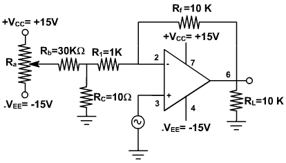
Ra = 10 kΩ potentiometer
Rb = 30 kΩ
Rc = 10Ω.The final circuit, which also includes the pin connections for the µA 715, shown in fig. 4.
Fig. 4