Series Regulators:
Voltage regulators may be classified as series regulators or shunt regulators. Improvements in performance of voltage regulators are possible using the series regulator. Fig. 3 shows a functional block diagram of the series type voltage regulator.
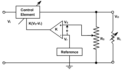
Fig. 3
The control element is a device which is in series with load and supply and its operating state adjusts as necessary to maintain a constant voltage Vo. A measuring circuit produces a feedback voltage proportional to Vo and this voltage is compared with a reference voltage. The output of the comparator circuit is the control signal that adjusts the operating state of the control element. If Vo decreases, due to increased in load, then the comparator produces a output that causes to control element to increase the output voltage.
The amplifier is of the differential input type; one input is Vs, while the other is Vr, a constant reference voltage. The reference may be a Zener diode or a dry cell. The amplifier output is proportional to the difference between its two inputs; this difference is called the error signal and may be expressed as follows:
e = VS -Vr
The amplifier multiplies the error by a constant K, yielding an appropriate signal to the control element. The function of the signal is to increase or decrease the effective resistance of the control element, depending on whether VO is too high or too low, respectively.
For example, if VO should increase, the error voltage e' also increases. The amplifier's output therefore increase; this causes the resistance of the control element to increase, therefore reducing the load current and load voltage. Note that the original increase in VO caused the circuit to act in such a manner as to decrease V O . It is because of this negative feedback that we are able to achieve control over the load voltage.
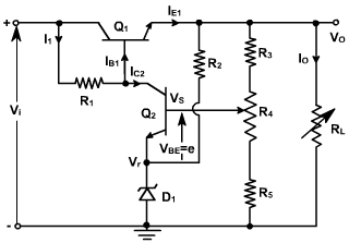
A circuit that operates on the above principle is shown in fig. 4. R3, R4, and R5 make up the sampling network. The current through the sampling network must be sufficiently large that, whatever current the base of Q2 draws, the loading on the voltage divider is negligible and VO remains an accurate sample to VO.
Fig. 4
It is possible to simply eliminate R3 and R5 and leave only R4, but there is the danger that in setting the potentiometer one will go to either extreme, in which case the transistor may be damaged. None of the transistor is critical; R4 is variable to allow setting of the output voltage.
The sample voltage Vs is applied to the base of Q2, while the reference voltage Vr, which is provided by Zener diode D1, is applied to the emitter. R2 sets the Zener current; in addition to ensuring that the Zener operates in the breakdown region, the Zener's temperature coefficient, which is both voltage- and current-dependent, may be controlled by an appropriate selection of current through R2. This way the Zener's temperature coefficient (usually positive) may be used to cancel the transistor's VBE temperature dependence (usually negative).
The error voltage is Vs -Vr, or simply VBE. Q2 yields an output current (IC2) which is proportional to this error. At junction A the following expression may be written
IC2 + IB1 = I1
If I1 is constant, changes in IC2 yield equal but opposite changes in IB1; that is, if IC2 rises, IB1 drops. Changes in IB1 are amplified by Q1 to yield corresponding changes in IE1 and IO. As the current through it changes, Q1 appears as a variable resistor whose resistance depends on the control current IB1. If IB1 drops, the resistance of Q1 increases, allowing less current to flow through the load.
It is important to note that is type of corrective action is effective only as long as I1 remains reasonably constant. This is to ensure that IB1 changes mainly in response to variations in IC2 (which are due to the error signal). If I1 is not constant, it is possible for IB1 (and hence IO and VO) to change in response to I1 variations which do not reflect conditions in the load circuit.