Active Half Wave Rectifier:
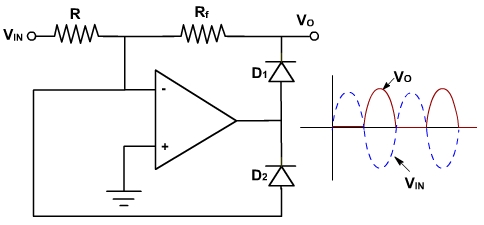
The Active half wave rectifier is shown in fig. 8.
 |
 |
|---|---|
| Fig. 8 | Fig. 9 |
If vin is positive then output of the OPAMP becomes negative (the non inverting terminal is grounded). Thus diode D2 conducts and provides a negative feedback. Because of the feedback through D2 a virtual ground exists at the input. Thus diode D1 acts as open circuit. The output voltage under this condition is given by
vo = v - = 0.
If vin goes negative, then output of the OPAMP becomes positive. Thus D1 is conducting and D2 is off. Thus, the circuit behaves as an inverting amplifier. The output of the circuit is given by
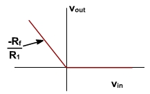
The resultant output voltage will be positive. If v in is a sinusoid, the circuit performs half wave rectification. The transfer characteristic of the half wave active rectifier is shown in fig. 9. The output does not depend upon the diode forward voltage (vd). Thus, because of the high open loop gain of the OPAMP, the feedback acts to cancel the diode turn-on (forward) voltage. This leads to improved performance since the diode more closely approximates the ideal device.
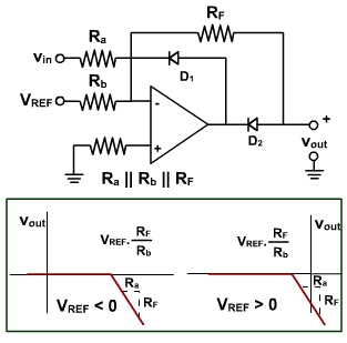
Axis Shifting of the Half Wave Rrectifier:
The half wave rectified output waveform can be shifted along the vin axis. This is done by using a reference voltage added to the input voltage of the rectifier as shown in fig. 10. This termed axis shifting. It adds or subtracts a fixed dc voltage to the input signal. This process shifts the diode turn-on voltage point. If a negative reference voltage, VREF, is applied to the circuit, the diode turns on when the input voltage is still positive. This shifts the vout/ vin transfer characteristic to the right. If a positive reference voltage is applied, the vout/ vin transfer characteristic shifts to the left. These shifted characteristics are shown in fig. 10.
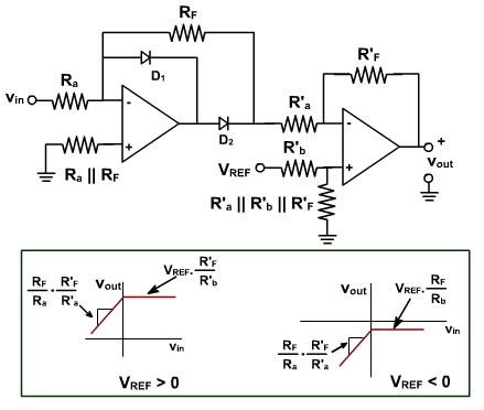
Fig. 10 Fig. 11 The input-output voltage characteristics can also be shifted up or down. This is termed level shifting and is accomplished by adding a second OPAMP with a reference voltage added to the negative input terminal as shown in fig. 11.