Design of Series Voltage Regulator:
Fig. 1 shows the basic circuit of a series voltage regulator. The operation of this regulator has been discussed in previous lecture. It consists of series (pass) transistor to control the output voltage.
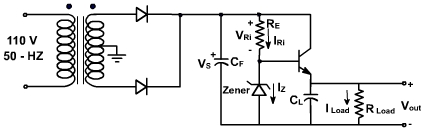
Fig. 1
The circuit can be designed taking two extreme operating conditions,
- VS max, IZ max, I load min / β
- VS min, IZ min, I load max / β
We calculate R s for both conditions and since R si is constant, we equate these two expressions as in Equation E-1.
(E-1)
A design guideline that set IZ min = 0.1 I Z max. Then we equate the expressions for Equation (E-1) to obtain,
(E-2)
Solving for IZ max, we obtain,
(E-3)
We estimate the load resistance by taking the ratio of the minimum source voltage to the maximum load current. Since R load is large and in parallel, it can be ignored. This is the worst case since it represents the smallest load and therefore the maximum load current.
(E-4)
The output filter capacitor size can be estimated according to the permissible output voltage variation and ripple voltage frequency and is given by
(E-5)
Since the voltage gain of an EF amplifier is unity, the output voltage of teh regulated power supply is,
Vload=VZ - VBE (E-6)
The percent regulation of the power supply is given by
(E-7)