HFET (hetrojunction FET) OR HEMT -high electron mobility transistor or  (two dimensional electron gas(2DEG))or MODFET (two dimensional electron gas(2DEG))or MODFET
A potential is formed at junction of two dissimilar semiconductors(AlGaAs/GaAs), where  is higher than the occupation levels of the electrons in the conduction band. is higher than the occupation levels of the electrons in the conduction band.
The electrons accumulated in this potential well and form a sheet of electron similar to the inversion layer in a MOS structure. The thickness of this sheet is  10nm, smaller than the De-broglie wavelength of the electron in that material. This sheet of free electrons behaves like free atoms in a gas and hence it is called electron gas.. 10nm, smaller than the De-broglie wavelength of the electron in that material. This sheet of free electrons behaves like free atoms in a gas and hence it is called electron gas..
In this structure  has been observed. has been observed.
This structure is similar to FET with 2DEG(Two Dimentional Electron Gas )as channel.
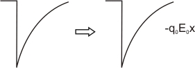
Application of a bias voltage to gate modulates charges in the 2DEG and thus channel conducts current, this is similar to FET which is faster than MESFET operation. The formation of 2DEG is shown in Fig 17.1
|