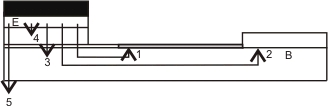
Components of the Base currents
The various components of the Base currents are shown in Fig 16.3, they are
. Back injection of holes
. Extrinsic base surface recombination current.
. Base contact surface recombination current
. Bulk recombination current in Base layer
. Depletion region recombination current in B-E depletion region.
Bulk recombination current in the base region (I Bbulk ) is the dominant base current and the current gain is given by
Where,  is the minority electron recombination lifetime in Base and is the minority electron recombination lifetime in Base and  is the minority carrier transit time in Base. is the minority carrier transit time in Base.
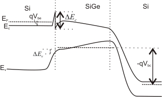
Now  when the Base is too thin. when the Base is too thin.
 can be decreased by an E field in base arising due to the linearly grading the bandgap in the Base region. can be decreased by an E field in base arising due to the linearly grading the bandgap in the Base region.
A linearly graded Si/SiGe HBT is shown in Fig 16.4
The Poisson Equation is given by
Base-Collector junction where the Base doping is greater than the Collector Doping the depletion region is mostly inside the Collector, where the Electric field is high and electrons travel mostly with saturation velocity.
The electron carrier concentration
The electron carrier concentration inside the collector is given by
 is the Collector current density. is the Collector current density.
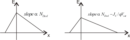
Thus the Electric field in Base-Collector depletion region is given by
.
When  is small is small  , ,
where N C is the Collector doping concentration
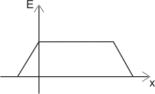
As  increases increases  slope becomes more negative as shown in Fig 16.5 slope becomes more negative as shown in Fig 16.5
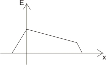
While the current density increases and the area under the field profile should remain constant the depletion region thickness would continue to increase until it reaches x= X c as shown in Fig 16.6
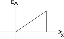
As the current density increases to a level such that x=X c , the net charge inside the junction becomes zero and the field profile is constant as shown in Fig 16.7
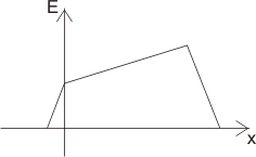
When J c increases further such that x>X c the net charge inside the junction becomes negative, the electric field takes negative values as shown in Fig 16.8
When there is no more field to prevent holes from spilling, base pushout or Kirk effect occurs as shown in Fig 16.9 The current gain decreases as the transit time associated with the thickened base layer increases
Emitter-Collector transit time
Emitter-Collector transit time is
Where
 is the time required to change the base potential by charging the capacitances is the time required to change the base potential by charging the capacitances  (B-E junction capacitance) and (B-E junction capacitance) and  (B-C junction capacitance) through the differential Base-Emitter junction resistance. (B-C junction capacitance) through the differential Base-Emitter junction resistance.
is the base transit time.
 is the transit time through B-C depletion region and is the transit time through B-C depletion region and
 is the Collector charging time is the Collector charging time
Hence the cut-off frequency is
|