QUANTUM WELL : PICTURE
It can be seen that if the temperature is high(seldom encountered) or the applied field (VDS) is high, the electrons are excited to high energies and may escape from the triangular well. It may also be scattered into conduction band of the barrier(spatial transfer) and the carriers would be lost from the channel. To avoid this a quantum well may be introduced at the interface.
Actually in this case we work at several possibilities of hetrostructures.
Charge transfer occurs leading to a conducting channel within single quantum well or multiple quantum well. The energies of the electrons are quantized in the step like density of states. Therefore many carriers can be put in the channel with a narrower dispersion of energies.
Electron wave inside well is
 This is Kane model. This is Kane model.
Where x is the growth direction and k is the transverse electron wave vector.
 block wave form and block wave form and  is the envelope wave function which is the solution of is the envelope wave function which is the solution of
Where  is the effective mass, is the effective mass,  is the potential and is the potential and  is the confinement energy of carriers. is the confinement energy of carriers.
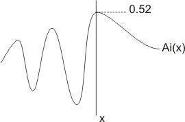
Boundary conditions are  should be continuous at the interfaces. The triangular potential well is shown in Fig 17.1 should be continuous at the interfaces. The triangular potential well is shown in Fig 17.1
The triangular quantum well Potential  is linear for is linear for  and and  at x = 0 at x = 0
The Schrödinger equation is
The boundary condition is
The above equation has two independent solutions.
One solution that is nonsingular at  is AIRY function (Ai), so the resulting wave function is is AIRY function (Ai), so the resulting wave function is
 as shown in Fig 17.2 as shown in Fig 17.2
The quantized energy levels are
Where,  is the nth zero of Ai(x), hence is the nth zero of Ai(x), hence
So
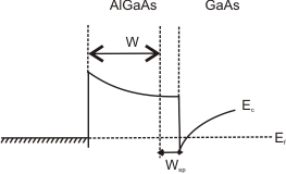
The basic idea of HFET or HEMT also known as MODFET- Modulation Doped Field Effect Transistor is that at equilibrium charge transfer occurs at the heterojunction to equalize the Fermi level on both side. Doping the N side gives wide base. Electrons are transferred to the GaAs side until an equilibrium is reached, this occurs because electron transfer raises the Fermi level on the GaAs side due to filling of the conduction band by electrons and also raises the electrostatic potential of the interface region because of the more numerous ionizer donors in the AlGaAs side. This charge transfer effect makes possible an old dream of semiconductor technologist, ie getting conducting electrons in a high mobility, High purity semiconductor without having to introduce mobility limiting donor impurities.
The various charge transfer mechanisms in heterojunctions are
- Electric charges and field near the interface determine the energy band bendings in the barrier and in conducting channel.
- The quantum calculation of the electron energy levels in the channel determines the confined conduction band levels
- The thermodynamic equilibrium conduction determine the density of transferred electrons.
Assuming that before the charge transfer the potential is flat band. After charge transfer of  electrons the electric field in the potential well created can be taken as constant to first order and is given by electrons the electric field in the potential well created can be taken as constant to first order and is given by
Gauss' Electrostatic potential is given by
Hence the Schrödinger equation for the electron envelope wave function is
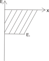
The energy level in infinite triangular potential well for the ground state  is is
Where  and is usually determined experimentally. and is usually determined experimentally.
As charge transfer increases, potential created by transferred electrons also increases, leading to the lowering of the bottom of the Conduction . A 2DEG is formed when the Conduction band goes below the Fermi level, hence we get
and the energy in channel is given by 
In AlGaAs Fermi energy level is pushed downwards by electrostatic potential  built up at the interface, where built up at the interface, where
Where W is the width of depletion region (Vdep ) in AlGaAs
Where  is the donor on AlGaAs is the donor on AlGaAs
Calculating energies from the bothom of Conduction Band, we get
and
Where  is the donor binding energy in AlGaAs. is the donor binding energy in AlGaAs.
The donor concentration  is equal to is equal to  i.e, the number of electron transferred. i.e, the number of electron transferred.
Hence we have
From the above equation NS can be calculated if the other parameters are known. The Fermi level is determined empirically by the model given by
In practice undoped AlGaAs spacer layer of thickness  is used to separate Donor atom from channel electrons (2DEG) to prevent coloumb interactions resulting in an increased mobility is used to separate Donor atom from channel electrons (2DEG) to prevent coloumb interactions resulting in an increased mobility  is decreased as shown in Fig 17.2 is decreased as shown in Fig 17.2
The charge in the conduction band is
Where
We have calculated the 2DEG charge density N S and it can be related to the gate voltage  by by
 with with 
|
Where ,  is the 2DEG capacitance per unit area as given by is the 2DEG capacitance per unit area as given by
Where  and is usually determined experimentally. and is usually determined experimentally.
As charge transfer increases, potential created by transferred electrons also increases, leading to the lowering of the bottom of the Conduction . A 2DEG is formed when the Conduction band goes below the Fermi level, hence we get
and the energy in channel is given by 
In AlGaAs Fermi energy level is pushed downwards by electrostatic potential  built up at the interface, where built up at the interface, where
Where W is the width of depletion region (  ) in AlGaAs ) in AlGaAs
Where  is the donor on AlGaAs is the donor on AlGaAs
Calculating energies from the bothom of Conduction Band, we get
Where  is the distance of the centroid of 2DEG from x = 0 as shown in Fig 17.3 and is usually is the distance of the centroid of 2DEG from x = 0 as shown in Fig 17.3 and is usually
Again the threshold voltage or pinch off voltage is given by
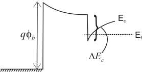
Where  is the Schottky barrier height on the donor layer as shown in Fig 17.4 is the Schottky barrier height on the donor layer as shown in Fig 17.4
At room temp  also modulates the bound carrier density in Donor layer and free electron in Donor layer. also modulates the bound carrier density in Donor layer and free electron in Donor layer.
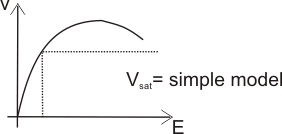
For a simplest model  is so large that all electrons in 2DEG channel move with is so large that all electrons in 2DEG channel move with  independent of independent of  as shown in Fig 17.5 and as shown in Fig 17.5 and 
Where  is the electron density per surface area and is given by is the electron density per surface area and is given by  , z is the gate width and , z is the gate width and  is the gate length. is the gate length.
The transconductance is
So we have
 Simplest model. Simplest model.
With  we have we have  and with and with  we have we have 
The voltage in the channel  and the current is given by and the current is given by
Hence current is given by
Where  is the position of entrance to channel on the source side. is the position of entrance to channel on the source side.
The saturation current is the current for which field on the drain side at  just reaches just reaches  is is
Where,  is the source resistance is the source resistance
For  we get we get |
a linear behavior for a short highly conductive channel. The I-V characteristic is shown in Fig 17.6
for  we get we get
|